 |
||||||||||||||||||||||||||||||||||||||||||||
| • Two High-Accuracy DAC Channels - 12-Bit Accuracy Without Adjustment - ±1 LSB INL Buffered Voltage Output - Monotonic Over All Operating Conditions - Independent Mode Settings for Each DAC |
||||||||||||||||||||||||||||||||||||||||||||
| • Three Precision Selectable Internal References - 2.048V, 2.500V, or 4.096V |
||||||||||||||||||||||||||||||||||||||||||||
| • Internal Output Buffer - Rail-to-Rail Operation with External Reference - 4.5µs Settling Time - Outputs Directly Drive 2kI Loads |
||||||||||||||||||||||||||||||||||||||||||||
| • Small 5mm x 3mm 10-Pin µMAX or Ultra-Small3mm x 3mm 10-Pin TDFN Package |
||||||||||||||||||||||||||||||||||||||||||||
| • Wide 2.7V to 5.5V Supply Range |
||||||||||||||||||||||||||||||||||||||||||||
| • Separate 1.8V to 5.5V VDDIO Power-Supply Input |
||||||||||||||||||||||||||||||||||||||||||||
| • Fast 400kHz I2C-Compatible, 2-Wire SerialInterface |
||||||||||||||||||||||||||||||||||||||||||||
| • Power-On-Reset to Zero-Scale DAC Output |
||||||||||||||||||||||||||||||||||||||||||||
| • CLR For Asynchronous Control |
||||||||||||||||||||||||||||||||||||||||||||
| • Three Software-Selectable Power-Down OutputImpedances - 1kI, 100kI, or High Impedance |
||||||||||||||||||||||||||||||||||||||||||||
| • Low 350µA Supply Current at 3V VDD |
||||||||||||||||||||||||||||||||||||||||||||
| CATALOG | ||||||||||||||||||||||||||||||||||||||||||||
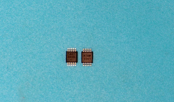
| MAX5802BAUB+ COUNTRY OF ORIGIN |
||||||||||||||||||||||||||||||||||||||||||||
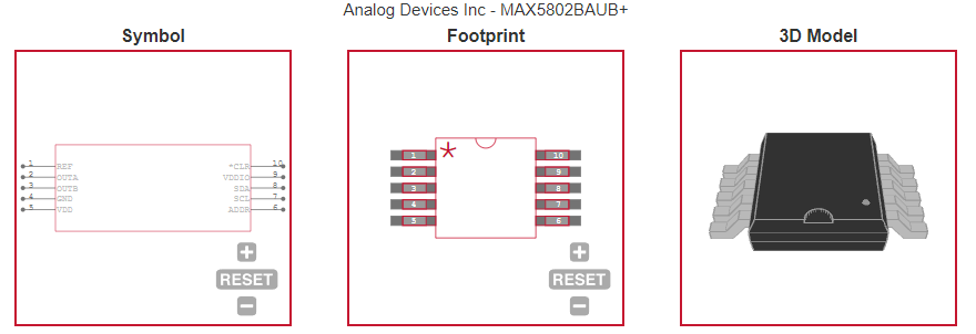
| MAX5802BAUB+ PARAMETRIC INFO |
||||||||||||||||||||||||||||||||||||||||||||
| MAX5802BAUB+ PACKAGE INFO |
||||||||||||||||||||||||||||||||||||||||||||
| MAX5802BAUB+ MANUFACTURING INFO |
||||||||||||||||||||||||||||||||||||||||||||
| MAX5802BAUB+ PACKAGING INFO |
||||||||||||||||||||||||||||||||||||||||||||
| MAX5802BAUB+ ECAD MODELS |
||||||||||||||||||||||||||||||||||||||||||||
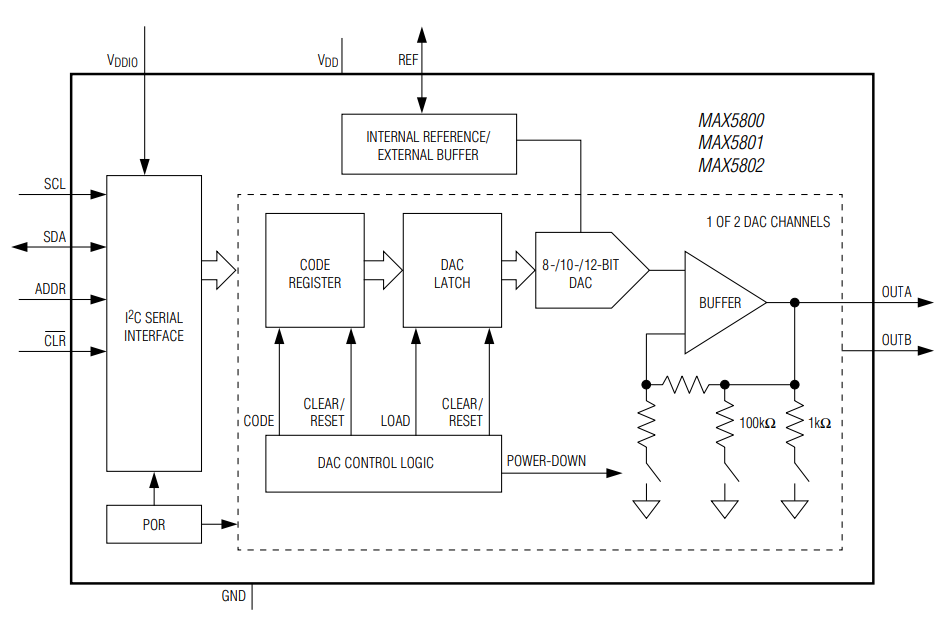
| MAX5802BAUB+ FUNCTIONAL BLOCK DIAGRAM |
||||||||||||||||||||||||||||||||||||||||||||
| MAX5802BAUB+ APPLICATIONS |
||||||||||||||||||||||||||||||||||||||||||||
| COUNTRY OF ORIGIN |
||||||||||||||||||||||||||||||||||||||||||||
| Thailand |
||||||||||||||||||||||||||||||||||||||||||||
| PARAMETRIC INFO |
||||||||||||||||||||||||||||||||||||||||||||
|
||||||||||||||||||||||||||||||||||||||||||||
| PACKAGE INFO |
||||||||||||||||||||||||||||||||||||||||||||
|
||||||||||||||||||||||||||||||||||||||||||||
| MANUFACTURING INFO |
||||||||||||||||||||||||||||||||||||||||||||
|
||||||||||||||||||||||||||||||||||||||||||||
| PACKAGING INFO |
||||||||||||||||||||||||||||||||||||||||||||
|
||||||||||||||||||||||||||||||||||||||||||||
| ECAD MODELS |
||||||||||||||||||||||||||||||||||||||||||||
 |
||||||||||||||||||||||||||||||||||||||||||||
| FUNCTIONAL BLOCK DIAGRAM |
||||||||||||||||||||||||||||||||||||||||||||
 |
||||||||||||||||||||||||||||||||||||||||||||
| APPLICATIONS |
||||||||||||||||||||||||||||||||||||||||||||
| • Programmable Voltage and Current Sources |
||||||||||||||||||||||||||||||||||||||||||||
| • Gain and Offset Adjustment |
||||||||||||||||||||||||||||||||||||||||||||
| • Automatic Tuning and Optical Control |
||||||||||||||||||||||||||||||||||||||||||||
| • Power Amplifier Control and Biasing |
||||||||||||||||||||||||||||||||||||||||||||
| • Process Control and Servo Loops |
||||||||||||||||||||||||||||||||||||||||||||
| • Portable Instrumentation |
||||||||||||||||||||||||||||||||||||||||||||
| • Data Acquisition |
||||||||||||||||||||||||||||||||||||||||||||