|
|
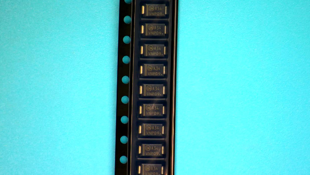
• Small Compact Surface Mountable Package with J−Bent Leads
|
• Rectangular Package for Automated Handling
|
• Highly Stable Oxide Passivated Junction
|
• Very Low Forward Voltage Drop
|
• Guardring for Stress Protection
|
• NRVBA Prefix for Automotive and Other Applications Requiring Unique Site and Control Change Requirements; AEC−Q101 Qualified and PPAP Capable*
|
• These Devices are Pb−Free, Halogen Free/BFR Free and are RoHS Compliant
|
|
| CATALOG |
MBRA340T3G COUNTRY OF ORIGIN
|
MBRA340T3G PARAMETRIC INFO
|
MBRA340T3G PACKAGE INFO
|
MBRA340T3G MANUFACTURING INFO
|
MBRA340T3G PACKAGING INFO
|
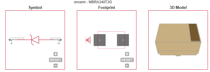
MBRA340T3G ECAD MODELS
|
|
COUNTRY OF ORIGIN
|
China
|
Viet Nam
|
Malaysia
|
|
PARAMETRIC INFO
|
| Type |
Schottky Diode |
| Configuration |
Single |
| Maximum DC Reverse Voltage (V) |
40 |
| Material |
Si |
| Peak Reverse Repetitive Voltage (V) |
40 |
| Maximum Continuous Forward Current (A) |
3 |
| Average Rectified Forward Current (A) |
3 |
| Maximum Junction Ambient Thermal Resistance |
81°C/W |
| Peak Forward Voltage (V) |
0.45 |
| Peak Non-Repetitive Surge Current (A) |
100 |
| Peak Reverse Current (uA) |
300 |
| Operating Junction Temperature (°C) |
-55 to 150 |
| Minimum Storage Temperature (°C) |
-55 |
| Maximum Storage Temperature (°C) |
150 |
| Minimum Operating Temperature (°C) |
-55 |
| Maximum Operating Temperature (°C) |
150 |
|
|
PACKAGE INFO
|
| Supplier Package |
SMA |
| Basic Package Type |
Lead-Frame SMT |
| Pin Count |
2 |
| Lead Shape |
J-Lead |
| PCB |
2 |
| Tab |
N/R |
| Pin Pitch (mm) |
N/R |
| Package Length (mm) |
4.32 |
| Package Width (mm) |
2.6 |
| Package Height (mm) |
2 |
| Package Diameter (mm) |
N/R |
| Package Overall Length (mm) |
5.21 |
| Package Overall Width (mm) |
2.6 |
| Package Overall Height (mm) |
2.1 |
| Seated Plane Height (mm) |
2.1 |
| Mounting |
Surface Mount |
| Package Weight (g) |
N/A |
| Package Material |
Plastic |
| Package Description |
SMD Plastic Package |
| Package Family Name |
DO |
| Jedec |
DO-214AC |
| Package Outline |
Link to Datasheet |
| Maximum PACKAGE_DIMENSION_H |
2 |
| Minimum PACKAGE_DIMENSION_H |
1.92 |
| Maximum PACKAGE_DIMENSION_L |
4.57 |
| Minimum PACKAGE_DIMENSION_L |
4.06 |
| Maximum PACKAGE_DIMENSION_W |
2.92 |
| Minimum PACKAGE_DIMENSION_W |
2.29 |
| Maximum Diameter |
N/R |
| Minimum Diameter |
N/R |
| Maximum Seated_Plane_Height |
2.2 |
| Minimum Seated_Plane_Height |
1.97 |
|
|
MANUFACTURING INFO
|
| MSL |
1 |
| Maximum Reflow Temperature (°C) |
260 |
| Reflow Solder Time (Sec) |
30 |
| Number of Reflow Cycle |
3 |
| Standard |
N/A |
| Reflow Temp. Source |
Link to Datasheet |
| Maximum Wave Temperature (°C) |
N/R |
| Wave Solder Time (Sec) |
N/R |
| Wave Temp. Source |
Link to Datasheet |
| Lead Finish(Plating) |
Matte Sn annealed |
| Under Plating Material |
N/A |
| Terminal Base Material |
Cu Alloy |
| Shelf Life Period |
24 Month |
| Number of Wave Cycles |
N/R |
|
|
PACKAGING INFO
|
| Packaging Suffix |
T3 |
| Packaging |
Tape and Reel |
| Quantity Of Packaging |
5000 |
| Reel Diameter (in) |
13 |
| Reel Width (mm) |
12.4(Min) |
| Tape Pitch (mm) |
4 |
| Tape Width (mm) |
12 |
| Feed Hole Pitch (mm) |
4 |
| Hole Center to Component Center (mm) |
2 |
| Component Orientation |
Cathode At Sprocket Hole |
| Packaging Document |
Link to Datasheet |
| Tape Type |
Embossed |
|
|
| ECAD MODELS |
 |
| |