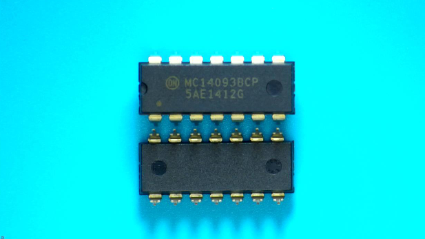
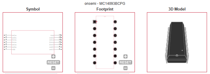
MC14093BCPG onsemi IC GATE NAND SCHMITT 4CH 14DIP

label:
2023/09/26 409


■ Supply Voltage Range = 3.0 Vdc to 18 Vdc
■ Capable of Driving Two Low−Power TTL Loads or One Low−Power Schottky TTL Load Over the Rated Temperature Range
■ Triple Diode Protection on All Inputs
■ Pin−for−Pin Compatible with CD4093
■ Can be Used to Replace MC14011B


CATALOG
MC14093BCPG COUNTRY OF ORIGIN
MC14093BCPG LIFECYCLE
MC14093BCPG PARAMETRIC INFO
MC14093BCPG PACKAGE INFO
MC14093BCPG MANUFACTURING INFO
MC14093BCPG PACKAGING INFO
MC14093BCPG ECAD MODELS


COUNTRY OF ORIGIN
Czechia
Indonesia
Slovakia
United States of America


LIFECYCLE
Obsolete
Oct 18,2013


PARAMETRIC INFO
Logic Family CD4000
Logic Function NAND
Number of Element Inputs 2-IN
Number of Element Outputs 1
Number of Elements per Chip 4
Number of Output Enables per Element 0
Number of Selection Inputs per Element 0
Process Technology CMOS
Input Type Schmitt Trigger
Minimum Operating Supply Voltage (V) 3
Maximum Operating Supply Voltage (V) 18
Typical Operating Supply Voltage (V) 3.3|5|9|12|15
Maximum High Level Output Current (mA) -4.2(Min)
Maximum Low Level Output Current (mA) 4.2(Min)
Minimum Operating Temperature (°C) -55
Maximum Operating Temperature (°C) 125
Supplier Temperature Grade Automotive
Maximum Propagation Delay Time @ Maximum CL (ns) 250@5V|100@10V|80@15V
Absolute Propagation Delay Time (ns) 250
Propagation Delay Test Condition (pF) 50
Maximum Quiescent Current (uA) 1
Typical Quiescent Current (uA) 0.0015


PACKAGE INFO
Supplier Package PDIP
Basic Package Type Through Hole
Pin Count 14
Lead Shape Through Hole
PCB 14
Tab N/R
Pin Pitch (mm) 2.54
Package Length (mm) 19.69(Max)
Package Width (mm) 7.11(Max)
Package Height (mm) 4.95(Max)
Package Diameter (mm) N/R
Package Overall Length (mm) 19.56(Max)
Package Overall Width (mm) 8.26(Max)
Package Overall Height (mm) 5.33(Max)
Seated Plane Height (mm) 5.33(Max)
Mounting Through Hole
Package Weight (g) N/A
Package Material Plastic
Package Description Plastic Dual In Line Package
Package Family Name DIP
Jedec MS-001AA
Package Outline Link to Datasheet


MANUFACTURING INFO
MSL N/R
Maximum Reflow Temperature (°C) N/R
Reflow Solder Time (Sec) N/R
Number of Reflow Cycle N/R
Maximum Wave Temperature (°C) 260
Wave Solder Time (Sec) 8
Wave Temp. Source Link to Datasheet
Lead Finish(Plating) Matte Sn annealed
Under Plating Material N/A
Terminal Base Material Cu Alloy
Number of Wave Cycles N/A


PACKAGING INFO
Packaging Tube
Quantity Of Packaging 500
Packaging Document Link to Datasheet


ECAD MODELS


Продукт RFQ