|
|
• UP Translates from a Low to a High Voltage or DOWN Translates from a High to a Low Voltage
|
• Input Threshold Can Be Shifted for TTL Compatibility
|
• No Sequencing Required on Power Supplies or Inputs for Power Up or Power Down
|
• 3 to 18 Vdc Operation for VDD and VCC
|
• Diode Protected Inputs to VSS
|
• Capable of Driving Two Low−Power TTL Loads or One Low−Power Schottky TTL Load Over the Rated Temperature Range
|
• These Devices are Pb−Free and are RoHS Compliant
|
|
| CATALOG |
MC14504BCPG COUNTRY OF ORIGIN
|
MC14504BCPG LIFECYCLE
|
MC14504BCPG PARAMETRIC INFO
|
MC14504BCPG PACKAGE INFO
|
MC14504BCPG MANUFACTURING INFO
|
MC14504BCPG PACKAGING INFO
|
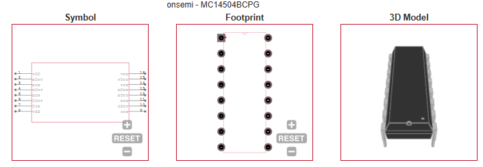
MC14504BCPG ECAD MODELS
|
|
COUNTRY OF ORIGIN
|
Indonesia
|
Slovakia
|
Japan
|
|
LIFECYCLE
|
Obsolete
Oct 18,2013
|
|
PARAMETRIC INFO
|
| Number of Channels |
6 |
| Channel Type |
Unidirectional |
| Logic Family |
4000 |
| Process Technology |
CMOS |
| Logic Function |
Voltage Level Shifter |
| Output Type |
Push-Pull |
| Translation |
CMOS/TTL to CMOS |
| Minimum Operating Temperature (°C) |
-55 |
| Maximum Operating Temperature (°C) |
125 |
| Minimum Storage Temperature (°C) |
-65 |
| Maximum Storage Temperature (°C) |
150 |
| Minimum Operating Supply Voltage (V) |
3 |
| Maximum Operating Supply Voltage (V) |
18 |
| Typical Operating Supply Voltage (V) |
3.3|5|9|12|15 |
| Maximum High Level Output Current (mA) |
-4.2(Min) |
| Maximum Low Level Output Current (mA) |
4.2(Min) |
| Maximum Quiescent Current (mA) |
5 |
| Maximum Propagation Delay Time @ Maximum CL (ns) |
550@5V@15V |
| Absolute Propagation Delay Time (ns) |
550 |
|
|
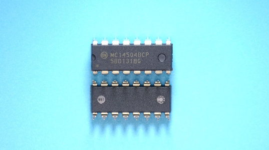
PACKAGE INFO
|
| Supplier Package |
PDIP |
| Basic Package Type |
Through Hole |
| Pin Count |
16 |
| Lead Shape |
Through Hole |
| PCB |
16 |
| Tab |
N/R |
| Pin Pitch (mm) |
2.54 |
| Package Length (mm) |
19.69(Max) |
| Package Width (mm) |
7.11(Max) |
| Package Height (mm) |
4.95(Max) |
| Package Diameter (mm) |
N/R |
| Package Overall Length (mm) |
19.69(Max) |
| Package Overall Width (mm) |
8.26(Max) |
| Package Overall Height (mm) |
5.33(Max) |
| Seated Plane Height (mm) |
5.33(Max) |
| Mounting |
Through Hole |
| Package Weight (g) |
N/A |
| Package Material |
Plastic |
| Package Description |
Plastic Dual In Line Package |
| Package Family Name |
DIP |
| Jedec |
MS-001BB |
| Package Outline |
Link to Datasheet |
|
|
MANUFACTURING INFO
|
| MSL |
N/R |
| Maximum Reflow Temperature (°C) |
N/R |
| Reflow Solder Time (Sec) |
N/R |
| Maximum Wave Temperature (°C) |
260 |
| Wave Solder Time (Sec) |
5 to 6 |
| Lead Finish(Plating) |
Matte Sn annealed |
| Under Plating Material |
N/A |
| Terminal Base Material |
CuFeAgZn |
| Number of Wave Cycles |
2 |
|
|
| PACKAGING INFO |
| Packaging |
Tube |
| Quantity Of Packaging |
500 |
| Packaging Document |
Link to Datasheet |
|
|
| ECAD MODELS |
 |
| |