|
|
• 1000 mA Output Current Capability
|
• Input Operating Voltage Range: 2.3V to 6.0V
|
• Adjustable Output Voltage Range: 0.8V to 5.0V(MCP1826 only)
|
| • Standard Fixed Output Voltages:- 0.8V, 1.2V, 1.8V, 2.5V, 3.0V, 3.3V, 5.0V
|
| • Other Fixed Output Voltage Options Available Upon Request |
| • Low Dropout Voltage: 250 mV Typical at 1000 mA |
| • Typical Output Voltage Tolerance: 0.5% |
| • Stable with 1.0 µF Ceramic Output Capacitor |
| • Fast Response to Load Transients |
| • Low Supply Current: 120 µA (typ) |
| • Low Shutdown Supply Current: 0.1 µA (typ)(MCP1826 only) |
| • Fixed Delay on Power Good Output(MCP1826 only) |
| • Short Circuit Current Limiting and Overtemperature Protection |
| • TO-263-5 (DDPAK-5), TO-220-5, SOT-223-5 Package Options (MCP1826) |
| • TO-263-3 (DDPAK-3), TO-220-3, SOT-223-3 Package Options (MCP1826S) |
| • Pass Automotive AEC-Q100 Reliability Testing |
|
| CATALOG |
| MCP1826S3302E/DB COUNTRY OF ORIGIN |
MCP1826S3302E/DB PARAMETRIC INFO
|
MCP1826S3302E/DB PACKAGE INFO
|
MCP1826S3302E/DB MANUFACTURING INFO
|
MCP1826S3302E/DB PACKAGING INFO
|
MCP1826S3302E/DB EACD MODELS
|
| MCP1826S3302E/DB APPLICATIONS |
|
| COUNTRY OF ORIGIN |
| Taiwan (Province of China) |
| China |
| Philippines |
|
PARAMETRIC INFO
|
| type |
LDO |
| Number of Outputs |
1 |
| Maximum Output Current (A) |
1(Min) |
| Minimum Operating Temperature (°C) |
-40 |
| Maximum Operating Temperature (°C) |
125 |
| Output Type |
Fixed |
| Output Voltage Range (V) |
1.8 to 10 |
| Regulation Condition Change In Load |
999mA |
| Junction to ambient |
62°C/W(Typ) |
| Junction to Case |
15°C/W(Typ) |
| Polarity |
Positive |
| Special Features |
Current Limit|Short Circuit Protection|Thermal Shutdown Protection |
| Process Technology |
CMOS |
| Load Regulation |
0.5%(Typ) |
| Line Regulation |
0.05%/V(Typ) |
| Maximum Quiescent Current (mA) |
0.22 |
| Maximum Dropout Voltage @ Current (V) |
0.4@1A |
| Minimum Input Voltage (V) |
2.3 |
| Maximum Input Voltage (V) |
6 |
| Output Voltage (V) |
3.3 |
| Typical Quiescent Current (mA) |
0.12 |
| Typical Dropout Voltage @ Current (V) |
0.25@1A |
| Accuracy (%) |
±0.5(Typ) |
| Supplier Temperature Rating |
car |
| Minimum Storage Temperature (°C) |
-65 |
| Maximum Storage Temperature (°C) |
150 |
| Typical Ground Current @ Full Load (mA) |
0.12 |
| Noise Spectral Density (uV/rtHz) |
2@1kHz |
| Typical PSRR (dB) |
60 |
| Typical Output Capacitance (uF) |
1 |
| Pass Element Type |
PMOS |
| Output Capacitor Type |
Ceramic|Tantalum|Aluminum |
|
|
PACKAGE INFO
|
| Supplier packaging |
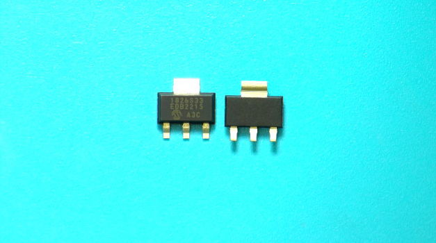
SOT-223 |
| Basic package type |
Lead-Frame SMT |
| Number of pins |
4 |
| Pin shape |
Gull-wing |
| PCB |
3 |
| ears |
ears |
| Pin spacing (mm) |
2.3 |
| Package length (mm) |
6.5 |
| Package width (mm) |
3.5 |
| Package height (mm) |
1.6 |
| Package diameter (mm) |
N/R |
| Package Overall Length (mm) |
6.5 |
| Package Overall Width (mm) |
7 |
| Package Overall Height (mm) |
1.8(Max) |
| Mounting surface height (mm) |
1.8(Max) |
| Install |
Surface Mount |
| Package weight (g) |
not applicable |
| Packaging materials |
Plastic |
| package instruction |
Small Outline Transistor |
| Package series name |
SOT |
| JEDEC |
TO-261AA |
| Package outline |
Link to datasheet |
|
|
MANUFACTURING INFO
|
| MSL |
3 |
| Maximum reflow temperature (°C) |
260 |
| Reflow soldering time (seconds) |
20 to 40 |
| Number of reflow cycles |
3 |
| standard |
J-STD-020C |
| Reflow temperature source |
Link to datasheet |
| Maximum wave soldering temperature (°C) |
N/R |
| Wave soldering time (seconds) |
N/R |
| Wave soldering temperature source |
Link to datasheet |
| Lead Finish(Plating) |
Matte Sn annealed |
| Plating materials |
not applicable |
| Terminal Base Material |
Cu Alloy |
| Shelf Life Period |
not applicable |
| Shelf Life Condition |
not applicable |
|
|
PACKAGING INFO
|
|
|
|
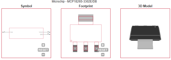
ECAD MODELS
|
|
|
| APPLICATIONS |
| • High-Speed Driver Chipset Power |
| • Networking Backplane Cards |
| • Notebook Computers |
| • Network Interface Cards |
| • Palmtop Computers |
| |