|
|
• SOT−23 Package Allows Either Two Separate Unidirectional Configurations or a Single Bidirectional Configuration
|
• Standard Zener Breakdown Voltage Range − 5.6 V to 47 V
|
• Peak Power − 24 or 40 W @ 1.0 ms (Unidirectional), per Figure 6 Waveform
|
• ESD Rating:− Class 3B (> 16 kV) per the Human Body Model− Class C (> 400 V) per the Machine Model
|
• ESD Rating of IEC61000−4−2 Level 4, ±30 kV Contact Discharge
|
• Maximum Clamping Voltage @ Peak Pulse Current
|
• Low Leakage < 5.0 A
|
• Flammability Rating UL 94 V−0
|
• SZ Prefix for Automotive and Other Applications Requiring Unique Site and Control Change Requirements; AEC−Q101 Qualified and PPAP Capable
|
• These Devices are Pb−Free and are RoHS Compliant
|
|
| CATALOG |
MMBZ27VALT1G COUNTRY OF ORIGIN
|
MMBZ27VALT1G PARAMETRIC INFO
|
MMBZ27VALT1G PACKAGE INFO
|
MMBZ27VALT1G MANUFACTURING INFO
|
MMBZ27VALT1G PACKAGING INFO
|
MMBZ27VALT1G ECAD MODELS
|
|
COUNTRY OF ORIGIN
|
China
|
|
PARAMETRIC INFO
|
| Type |
Zener |
| Direction Type |
Uni-Directional|Bi-Directional |
| Maximum Working Voltage (V) |
22 |
| Maximum Power Dissipation (mW) |
300 |
| Nominal Zener Voltage (V) |
27 |
| Configuration |
Dual Common Anode|Single |
| Maximum Clamping Voltage (V) |
40 |
| Maximum Reverse Leakage Current (uA) |
0.05 |
| Operating Junction Temperature (°C) |
-55 to 150 |
| Maximum Breakdown Voltage (V) |
28.35 |
| Number of Elements per Chip |
2 |
| Test Current (mA) |
1 |
| Peak Pulse Power Dissipation (W) |
40 |
| Maximum Peak Pulse Current (A) |
1 |
| Minimum Breakdown Voltage (V) |
25.65 |
| Minimum Operating Temperature (°C) |
-55 |
| Maximum Operating Temperature (°C) |
150 |
| Minimum Storage Temperature (°C) |
-55 |
| Maximum Storage Temperature (°C) |
150 |
|
|
PACKAGE INFO
|
| Supplier Package |
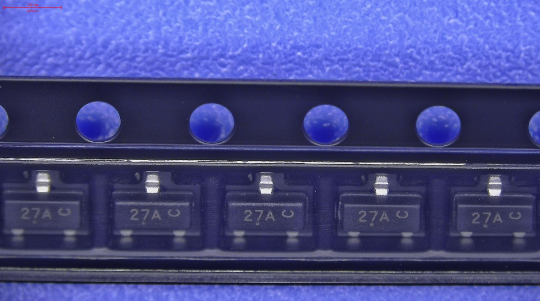
SOT-23 |
| Basic Package Type |
Lead-Frame SMT |
| Pin Count |
3 |
| Lead Shape |
Gull-wing |
| PCB |
3 |
| Tab |
N/R |
| Pin Pitch (mm) |
0.95 |
| Package Length (mm) |
2.9 |
| Package Width (mm) |
1.3 |
| Package Height (mm) |
0.94 |
| Package Diameter (mm) |
N/R |
| Package Overall Length (mm) |
2.9 |
| Package Overall Width (mm) |
2.4 |
| Package Overall Height (mm) |
1 |
| Seated Plane Height (mm) |
1 |
| Mounting |
Surface Mount |
| Package Weight (g) |
N/A |
| Package Material |
Plastic |
| Package Description |
Small Outline Transistor |
| Package Family Name |
SOT |
| Jedec |
TO-236AB |
| Package Outline |
Link to Datasheet |
|
|
MANUFACTURING INFO
|
| MSL |
1 |
| Maximum Reflow Temperature (°C) |
260 |
| Reflow Solder Time (Sec) |
30 |
| Number of Reflow Cycle |
3 |
| Standard |
N/A |
| Reflow Temp. Source |
Link to Datasheet |
| Maximum Wave Temperature (°C) |
N/R |
| Wave Solder Time (Sec) |
N/R |
| Lead Finish(Plating) |
Matte Sn annealed |
| Under Plating Material |
N/A |
| Terminal Base Material |
CuFeNi |
| Number of Wave Cycles |
N/R |
|
|
PACKAGING INFO
|
| Packaging Suffix |
T1 |
| Packaging |
Tape and Reel |
| Quantity Of Packaging |
3000 |
| Packaging Document |
Link to Datasheet |
|
|
| ECAD MODELS |
 |
| |