 |
|
• Four to six buck converters, depending on configuration
• Single/Dual phase/ parallel options
• DDR termination tracking mode option |
| • Boost regulator to 5.0 V output |
| • Six general purpose linear regulators |
| • Programmable output voltage, sequence, and timing |
| • OTP (one time programmable) memory for device configuration |
| • Coin cell charger and RTC supply |
| • DDR termination reference voltage |
| • Power control logic with processor interface and event detection |
| • I2C control |
| • Individually programmable ON, OFF, and standby modes |
|
| CATALOG |
| MMPF0100F0AEP COUNTRY OF ORIGIN |
| MMPF0100F0AEP PARAMETRIC INFO |
| MMPF0100F0AEP PACKAGE INFO |
| MMPF0100F0AEP MANUFACTURING INFO |
| MMPF0100F0AEP PACKAGING INFO |
| MMPF0100F0AEP ECAD MODELS |
| MMPF0100F0AEP FUNCTIONAL BLOCK DIAGRAM |
| MMPF0100F0AEP APPLICATIONS |
|
| COUNTRY OF ORIGIN |
| China |
| Malaysia |
| Korea (Republic of) |
|
| PARAMETRIC INFO |
| Function |
Application Processors |
| Input Voltage (V) |
2.8 to 4.5 |
| Switching Frequency (kHz) |
4000(Typ) |
| Minimum Operating Temperature (°C) |
-40 |
| Maximum Operating Temperature (°C) |
85 |
| Minimum Operating Supply Voltage (V) |
2.8 |
| Maximum Operating Supply Voltage (V) |
4.5 |
| Maximum Storage Temperature (°C) |
150 |
| Minimum Storage Temperature (°C) |
-65 |
| Supplier Temperature Grade |
Industrial |
|
| |
| PACKAGE INFO |
| Supplier Package |
HVQFN EP |
| Basic Package Type |
Non-Lead-Frame SMT |
| Pin Count |
56 |
| Lead Shape |
No Lead |
| PCB |
56 |
| Tab |
N/R |
| Pin Pitch (mm) |
0.5 |
| Package Length (mm) |
8 |
| Package Width (mm) |
8 |
| Package Height (mm) |
0.95(Max) |
| Package Diameter (mm) |
N/R |
| Package Overall Length (mm) |
8 |
| Package Overall Width (mm) |
8 |
| Package Overall Height (mm) |
1(Max) |
| Seated Plane Height (mm) |
1(Max) |
| Mounting |
Surface Mount |
| Package Material |
Plastic |
| Package Description |
Thermal Enhanced Very Thin Quad Flat Package, Exposed Pad |
| Package Family Name |
QFN |
| Package Outline |
Link to Datasheet |
|
| |
| MANUFACTURING INFO |
| MSL |
3 |
| Maximum Reflow Temperature (°C) |
260 |
| Reflow Solder Time (Sec) |
40 |
| Number of Reflow Cycle |
3 |
| Standard |
J-STD-020C |
| Reflow Temp. Source |
Link to Datasheet |
| Maximum Wave Temperature (°C) |
N/R |
| Wave Solder Time (Sec) |
N/R |
| Wave Temp. Source |
Link to Datasheet |
| Lead Finish(Plating) |
Matte Sn annealed |
| Under Plating Material |
Ag |
| Terminal Base Material |
Cu Alloy |
| Number of Wave Cycles |
N/R |
|
| |
| PACKAGING INFO |
| Packaging |
Tray |
| Quantity Of Packaging |
260(Min) |
|
| |
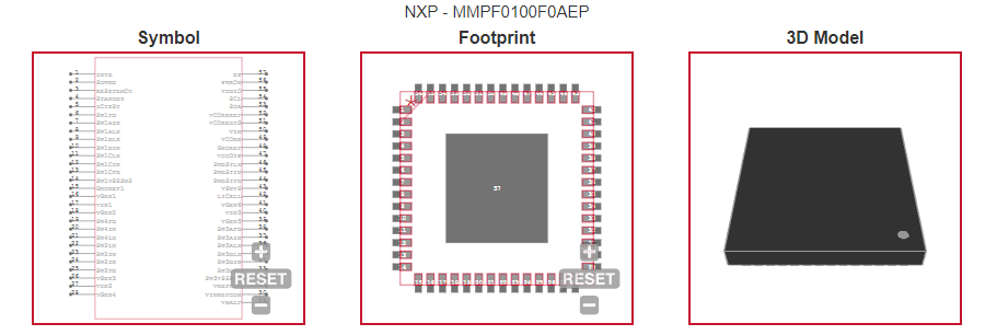
| ECAD MODELS |
 |
|
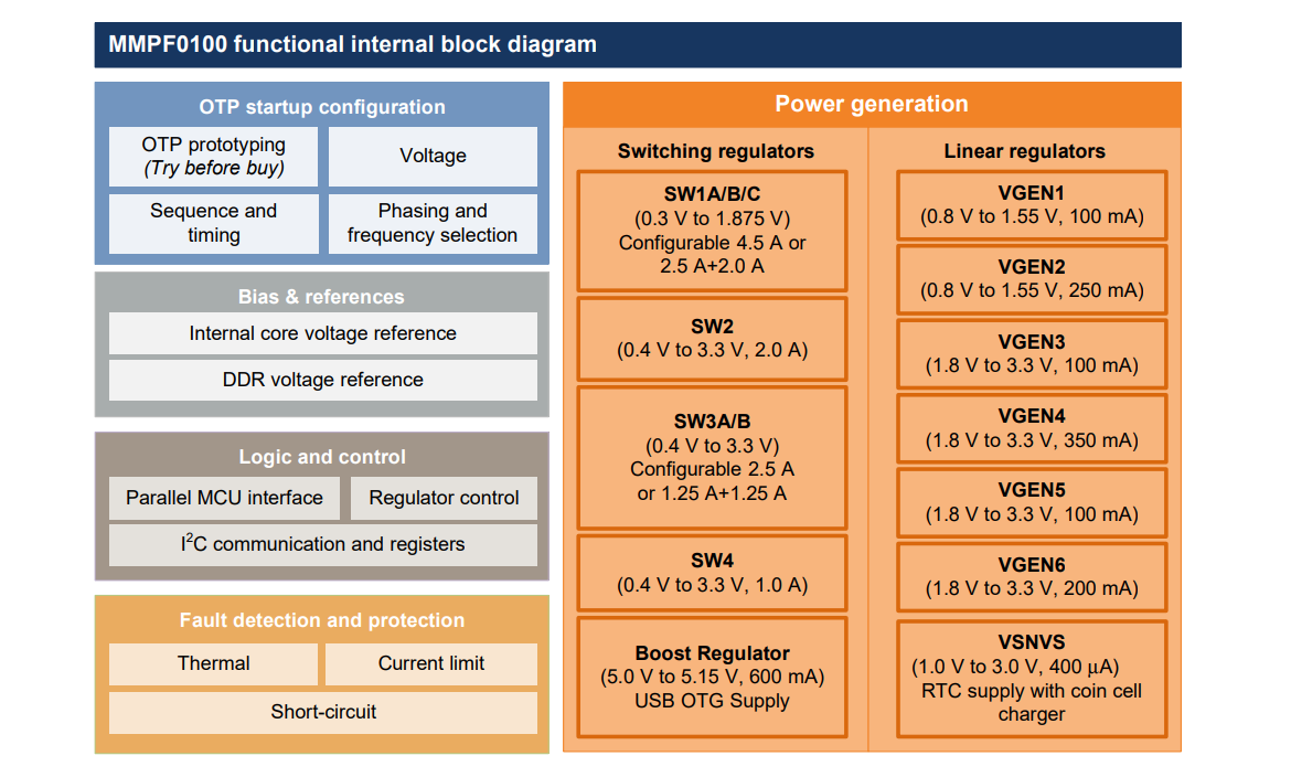
| FUNCTIONAL BLOCK DIAGRAM |
 |
|
| APPLICATIONS |
| • Tablets |
| • IPTV |
| • eReaders |
| • Set top boxes |
| • Industrial control |
| • Medical monitoring |
| • Home automation/ alarm/ energy management |
| |
|