 |
||||||||||||||||||||||||||||||||||||||||||||||||||||||||||||||||||||||||||||||
| • SPI-compatible serial bus interface |
||||||||||||||||||||||||||||||||||||||||||||||||||||||||||||||||||||||||||||||
| • Single and double transfer rate (STR/DTR) |
||||||||||||||||||||||||||||||||||||||||||||||||||||||||||||||||||||||||||||||
| • Clock frequency – 166 MHz (MAX) for all protocols in STR – 90 MHz (MAX) for all protocols in DTR |
||||||||||||||||||||||||||||||||||||||||||||||||||||||||||||||||||||||||||||||
| • Dual/quad I/O commands for increased throughput up to 90 MB/s |
||||||||||||||||||||||||||||||||||||||||||||||||||||||||||||||||||||||||||||||
| • Supported protocols in both STR and DTR – Extended I/O protocol – Dual I/O protocol – Quad I/O protocol |
||||||||||||||||||||||||||||||||||||||||||||||||||||||||||||||||||||||||||||||
| • Execute-in-place (XIP) |
||||||||||||||||||||||||||||||||||||||||||||||||||||||||||||||||||||||||||||||
| • PROGRAM/ERASE SUSPEND operations |
||||||||||||||||||||||||||||||||||||||||||||||||||||||||||||||||||||||||||||||
| • Volatile and nonvolatile configuration settings |
||||||||||||||||||||||||||||||||||||||||||||||||||||||||||||||||||||||||||||||
| • Software reset |
||||||||||||||||||||||||||||||||||||||||||||||||||||||||||||||||||||||||||||||
| • Additional reset pin for selected part numbers |
||||||||||||||||||||||||||||||||||||||||||||||||||||||||||||||||||||||||||||||
| • 3-byte and 4-byte address modes – enable memoryaccess beyond 128Mb |
||||||||||||||||||||||||||||||||||||||||||||||||||||||||||||||||||||||||||||||
| • Dedicated 64-byte OTP area outside main memory – Readable and user-lockable – Permanent lock with PROGRAM OTP command |
||||||||||||||||||||||||||||||||||||||||||||||||||||||||||||||||||||||||||||||
| • Erase capability – Bulk erase – Sector erase 64KB uniform granularity – Subsector erase 4KB, 32KB granularity |
||||||||||||||||||||||||||||||||||||||||||||||||||||||||||||||||||||||||||||||
| • Security and write protection – Volatile and nonvolatile locking and softwarewrite protection for each 64KB sector – Nonvolatile configuration locking – Password protection – Hardware write protection: nonvolatile bits(BP[3:0] and TB) define protected area size – Program/erase protection during power-up – CRC detects accidental changes to raw data |
||||||||||||||||||||||||||||||||||||||||||||||||||||||||||||||||||||||||||||||
| • Electronic signature – JEDEC-standard 3-byte signature (BB20h) – Extended device ID: two additional bytes identifydevice factory options |
||||||||||||||||||||||||||||||||||||||||||||||||||||||||||||||||||||||||||||||
| • JESD47H-compliant – Minimum 100,000 ERASE cycles per sector – Data retention: 20 years (TYP) |
||||||||||||||||||||||||||||||||||||||||||||||||||||||||||||||||||||||||||||||
| CATALOG | ||||||||||||||||||||||||||||||||||||||||||||||||||||||||||||||||||||||||||||||
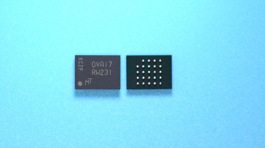
| MT25QU512ABB8E12-0AAT COUNTRY OF ORIGIN |
||||||||||||||||||||||||||||||||||||||||||||||||||||||||||||||||||||||||||||||
| MT25QU512ABB8E12-0AAT PARAMETRIC INFO |
||||||||||||||||||||||||||||||||||||||||||||||||||||||||||||||||||||||||||||||
| MT25QU512ABB8E12-0AAT PACKAGE INFO |
||||||||||||||||||||||||||||||||||||||||||||||||||||||||||||||||||||||||||||||
| MT25QU512ABB8E12-0AAT MANUFACTURING INFO |
||||||||||||||||||||||||||||||||||||||||||||||||||||||||||||||||||||||||||||||
| MT25QU512ABB8E12-0AAT PACKAGING INFO |
||||||||||||||||||||||||||||||||||||||||||||||||||||||||||||||||||||||||||||||
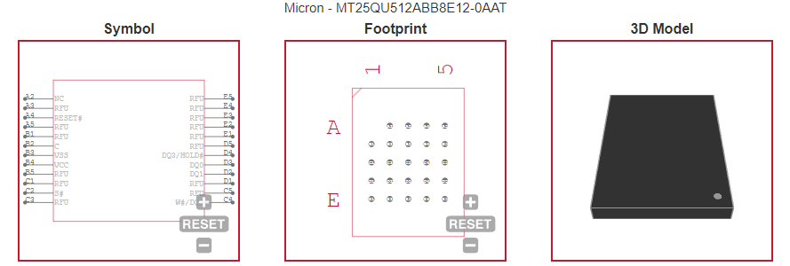
| MT25QU512ABB8E12-0AAT ECAD MODELS |
||||||||||||||||||||||||||||||||||||||||||||||||||||||||||||||||||||||||||||||
| COUNTRY OF ORIGIN |
||||||||||||||||||||||||||||||||||||||||||||||||||||||||||||||||||||||||||||||
| Taiwan (Province of China) |
||||||||||||||||||||||||||||||||||||||||||||||||||||||||||||||||||||||||||||||
| PARAMETRIC INFO |
||||||||||||||||||||||||||||||||||||||||||||||||||||||||||||||||||||||||||||||
|
||||||||||||||||||||||||||||||||||||||||||||||||||||||||||||||||||||||||||||||
| PACKAGE INFO |
||||||||||||||||||||||||||||||||||||||||||||||||||||||||||||||||||||||||||||||
|
||||||||||||||||||||||||||||||||||||||||||||||||||||||||||||||||||||||||||||||
| MANUFACTURING INFO |
||||||||||||||||||||||||||||||||||||||||||||||||||||||||||||||||||||||||||||||
|
||||||||||||||||||||||||||||||||||||||||||||||||||||||||||||||||||||||||||||||
| PACKAGING INFO |
||||||||||||||||||||||||||||||||||||||||||||||||||||||||||||||||||||||||||||||
|
||||||||||||||||||||||||||||||||||||||||||||||||||||||||||||||||||||||||||||||
| ECAD MODELS |
||||||||||||||||||||||||||||||||||||||||||||||||||||||||||||||||||||||||||||||
 |
||||||||||||||||||||||||||||||||||||||||||||||||||||||||||||||||||||||||||||||