 |
||||||||||||||||||||||||||||||||||||||||||||||||||||||||||||||||||||||||||||
| • SPI-compatible serial bus interface |
||||||||||||||||||||||||||||||||||||||||||||||||||||||||||||||||||||||||||||
| • 108 MHz (MAX) clock frequency |
||||||||||||||||||||||||||||||||||||||||||||||||||||||||||||||||||||||||||||
| • 2.7–3.6V single supply voltage |
||||||||||||||||||||||||||||||||||||||||||||||||||||||||||||||||||||||||||||
| • Dual/quad I/O instruction provides increasedthroughput up to 432 MHz |
||||||||||||||||||||||||||||||||||||||||||||||||||||||||||||||||||||||||||||
| • Supported protocols – Extended SPI, dual I/O, and quad I/O |
||||||||||||||||||||||||||||||||||||||||||||||||||||||||||||||||||||||||||||
| • Execute-in-place (XIP) mode for all three protocols – Configurable via volatile or nonvolatile registers – Enables memory to work in XIP mode directly after power-on |
||||||||||||||||||||||||||||||||||||||||||||||||||||||||||||||||||||||||||||
| • PROGRAM/ERASE SUSPEND operations |
||||||||||||||||||||||||||||||||||||||||||||||||||||||||||||||||||||||||||||
| • Continuous read of entire memory via a single command – Fast read – Quad or dual output fast read – Quad or dual I/O fast read |
||||||||||||||||||||||||||||||||||||||||||||||||||||||||||||||||||||||||||||
| • Flexible to fit application – Configurable number of dummy cycles – Output buffer configurable |
||||||||||||||||||||||||||||||||||||||||||||||||||||||||||||||||||||||||||||
| • Software reset |
||||||||||||||||||||||||||||||||||||||||||||||||||||||||||||||||||||||||||||
| • 64-byte, user-lockable, one-time programmable(OTP) dedicated area |
||||||||||||||||||||||||||||||||||||||||||||||||||||||||||||||||||||||||||||
| • Erase capability – Subsector erase 4KB uniform granularity blocks – Sector erase 64KB uniform granularity blocks – Full-chip erase |
||||||||||||||||||||||||||||||||||||||||||||||||||||||||||||||||||||||||||||
| • Write protection – Software write protection applicable to every64KB sector via volatile lock bit – Hardware write protection: protected area sizedefined by five nonvolatile bits (BP0, BP1, BP2,BP3, and TB) – Additional smart protections, available upon request |
||||||||||||||||||||||||||||||||||||||||||||||||||||||||||||||||||||||||||||
| • Electronic signature – JEDEC-standard 2-byte signature (BA18h) – Unique ID code (UID): 17 read-only bytes, including: • Two additional extended device ID (EDID)bytes to identify device factory options • Customized factory data (14 bytes) |
||||||||||||||||||||||||||||||||||||||||||||||||||||||||||||||||||||||||||||
| • Minimum 100,000 ERASE cycles per sector |
||||||||||||||||||||||||||||||||||||||||||||||||||||||||||||||||||||||||||||
| • More than 20 years data retention |
||||||||||||||||||||||||||||||||||||||||||||||||||||||||||||||||||||||||||||
| • Packages JEDEC standard, all RoHS compliant – F7 = V-PDFN-8 6mm x 5mm Sawn (MLP8 6mm x5mm) – F8 = V-PDFN-8 8mm x 6mm (MLP8 8mm x 6mm) – 12 = T-PBGA-24b05 6mm x 8mm – 14 = T-PBGA-24b05 6mm x 8mm, 4x6 ball array – SF = SOP2-16 300 mils body width (SO16W) – SE = SOP2-8 208 mils body width (SO8W) |
||||||||||||||||||||||||||||||||||||||||||||||||||||||||||||||||||||||||||||
| CATALOG | ||||||||||||||||||||||||||||||||||||||||||||||||||||||||||||||||||||||||||||
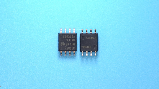
| N25Q128A13ESE40G COUNTRY OF ORIGIN |
||||||||||||||||||||||||||||||||||||||||||||||||||||||||||||||||||||||||||||
| N25Q128A13ESE40G LIFECYCLE |
||||||||||||||||||||||||||||||||||||||||||||||||||||||||||||||||||||||||||||
| N25Q128A13ESE40G PARAMETRIC INFO |
||||||||||||||||||||||||||||||||||||||||||||||||||||||||||||||||||||||||||||
| N25Q128A13ESE40G PACKAGE INFO |
||||||||||||||||||||||||||||||||||||||||||||||||||||||||||||||||||||||||||||
| N25Q128A13ESE40G MANUFACTURING INFO |
||||||||||||||||||||||||||||||||||||||||||||||||||||||||||||||||||||||||||||
| N25Q128A13ESE40G PACKAGING INFO |
||||||||||||||||||||||||||||||||||||||||||||||||||||||||||||||||||||||||||||
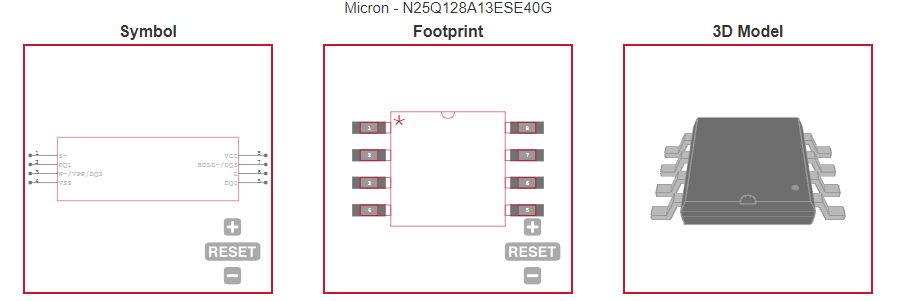
| N25Q128A13ESE40G ECAD MODELS |
||||||||||||||||||||||||||||||||||||||||||||||||||||||||||||||||||||||||||||
| COUNTRY OF ORIGIN |
||||||||||||||||||||||||||||||||||||||||||||||||||||||||||||||||||||||||||||
| China |
||||||||||||||||||||||||||||||||||||||||||||||||||||||||||||||||||||||||||||
| LIFECYCLE |
||||||||||||||||||||||||||||||||||||||||||||||||||||||||||||||||||||||||||||
| Obsolete Dec 05,2017 |
||||||||||||||||||||||||||||||||||||||||||||||||||||||||||||||||||||||||||||
| PARAMETRIC INFO |
||||||||||||||||||||||||||||||||||||||||||||||||||||||||||||||||||||||||||||
|
||||||||||||||||||||||||||||||||||||||||||||||||||||||||||||||||||||||||||||
| PACKAGE INFO |
||||||||||||||||||||||||||||||||||||||||||||||||||||||||||||||||||||||||||||
|
||||||||||||||||||||||||||||||||||||||||||||||||||||||||||||||||||||||||||||
| MANUFACTURING INFO |
||||||||||||||||||||||||||||||||||||||||||||||||||||||||||||||||||||||||||||
|
||||||||||||||||||||||||||||||||||||||||||||||||||||||||||||||||||||||||||||
| PACKAGING INFO |
||||||||||||||||||||||||||||||||||||||||||||||||||||||||||||||||||||||||||||
|
||||||||||||||||||||||||||||||||||||||||||||||||||||||||||||||||||||||||||||
| |
||||||||||||||||||||||||||||||||||||||||||||||||||||||||||||||||||||||||||||
| ECAD MODELS | ||||||||||||||||||||||||||||||||||||||||||||||||||||||||||||||||||||||||||||
 |
||||||||||||||||||||||||||||||||||||||||||||||||||||||||||||||||||||||||||||
| |