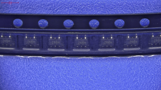
 |
|
• Broad Vcc Operating Range: 1.65 V to 5.5 V
|
| • Rail-to-Rail Signal Handling |
| • Power Down High-Impedance Inputs/Outputs |
| • 5Ω Switch Connection between Two Ports |
| • Minimal Propagation Delay through the Switch |
| • Low lcc |
| • Zero Bounce in Flow-Through Mode |
| • Control Input Compatible with CMOS Input Levels |
| • Ultra-Small MicroPak TM Packages |
| • Space-Saving SOT23 and SC70 Packages |
|
| CATALOG |
| NC7SZ66P5X COUNTRY OF ORIGIN |
| NC7SZ66P5X LIFECYCLE |
| NC7SZ66P5X PARAMETRIC INFO |
| NC7SZ66P5X PACKAGE INFO |
| NC7SZ66P5X MANUFACTURING INFO |
| NC7SZ66P5X PACKAGING INFO |
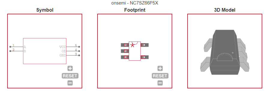
| NC7SZ66P5X ECAD MODELS |
|
| COUNTRY OF ORIGIN |
| China |
| Malaysia |
| Philippines |
| Thailand |
|
| LIFECYCLE |
Obsolete
Apr 01,2022 |
|
| PARAMETRIC INFO |
| Type |
Analog Switch |
| Number of Channels per Chip |
1 |
| Switch Architecture |
SPST |
| Polarity |
Non-Inverting |
| Maximum On Resistance Range (Ohm) |
60 to 80 |
| Configuration |
Single SPST |
| Number of Inputs per Chip |
1 |
| Function |
General |
| Number of Outputs per Chip |
1 |
| Logic Family |
SZ |
| Chip Enable Signals |
Yes |
| Maximum On Resistance (Ohm) |
60@1.8V |
| Maximum Propagation Delay Bus to Bus (ns) |
4.3@1.95V|1.2@2.7V|0.8@3.6V|0.3@5.5V@-40C to 85C |
| Maximum Turn-On Time (ns) |
7(Typ)@1.95V |
| Maximum Turn-Off Time (ns) |
9.2(Typ)@1.95V |
| Maximum Power Dissipation (mW) |
150 |
| Input Signal Type |
Single |
| Output Signal Type |
Single |
| Propagation Delay Test Condition (pF) |
50 |
| Maximum High Level Output Current (mA) |
128 |
| Switch Control Logic |
Active High |
| Switch Normal Position |
NO |
| Minimum Operating Temperature (°C) |
-40 |
| Maximum Operating Temperature (°C) |
85 |
| Power Supply Type |
Single |
| Minimum Single Supply Voltage (V) |
1.65 |
| Typical Single Supply Voltage (V) |
3|5 |
| Maximum Single Supply Voltage (V) |
5.5 |
|
| |
| PACKAGE INFO |
| Supplier Package |
SC-70 |
| Basic Package Type |
Lead-Frame SMT |
| Pin Count |
5 |
| Lead Shape |
Gull-wing |
| PCB |
5 |
| Tab |
N/R |
| Pin Pitch (mm) |
0.65 |
| Package Length (mm) |
2 |
| Package Width (mm) |
1.25 |
| Package Height (mm) |
1(Max) |
| Package Diameter (mm) |
N/R |
| Package Overall Length (mm) |
2 |
| Package Overall Width (mm) |
2.1 |
| Package Overall Height (mm) |
1.1(Max) |
| Seated Plane Height (mm) |
1.1(Max) |
| Mounting |
Surface Mount |
| Package Weight (g) |
N/A |
| Package Material |
Plastic |
| Package Description |
Small Outline Transistor |
| Package Family Name |
SOT |
| Jedec |
MO-203AA |
| Package Outline |
Link to Datasheet |
|
| |
| MANUFACTURING INFO |
| MSL |
1 |
| Maximum Reflow Temperature (°C) |
260 |
| Reflow Solder Time (Sec) |
30 |
| Number of Reflow Cycle |
3 |
| Standard |
IPC-1752 |
| Reflow Temp. Source |
Link to Datasheet |
| Maximum Wave Temperature (°C) |
N/R |
| Wave Solder Time (Sec) |
N/R |
| Lead Finish(Plating) |
Matte Sn annealed |
| Under Plating Material |
N/A |
| Terminal Base Material |
CuFeZnP |
|
| |
| PACKAGING INFO |
| Packaging Suffix |
X |
| Packaging |
Tape and Reel |
| Quantity Of Packaging |
3000 |
| Packaging Document |
Link to Datasheet |
|
| |
| ECAD MODELS |
 |
|

