|
|
• Ultra−High Speed: tPD = 3.6 ns (Typical) into 50 pF at 5 V VCC
|
• High Output Drive: ±24 mA at 3 V VCC
|
• Broad VCC Operating Range: 1.65 V to 5.5 V
|
| • Matches Performance of LCX when Operated at 3.3 V VCC
|
| • Power Down High−Impedance Inputs / Outputs |
| • Over−Voltage Tolerance Inputs Facilitate 5 V to 3 V Translation |
| • Proprietary Noise / EMI Reduction Circuitry |
| • Ultra−Small MicroPak™ Packages |
| • Space−Saving SC−88 Package |
| • These Devices are Pb−Free, Halogen Free/BFR Free and are RoHS Compliant |
|
| CATALOG |
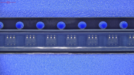
| NC7WZ17P6X COUNTRY OF ORIGIN |
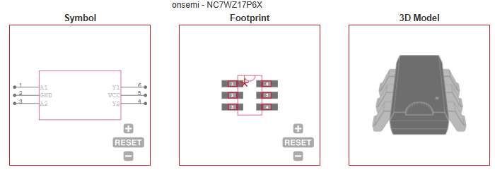
NC7WZ17P6X PARAMETRIC INFO
|
NC7WZ17P6X PACKAGE INFO
|
NC7WZ17P6X MANUFACTURING INFO
|
NC7WZ17P6X PACKAGING INFO
|
NC7WZ17P6X EACD MODELS
|
|
| COUNTRY OF ORIGIN |
| Philippines |
| Thailand |
| China |
| Malaysia |
|
PARAMETRIC INFO
|
| Process Technology |
CMOS |
| Logic Family |
WZ |
| Logic Function |
Schmitt Trigger Buffer |
| Input Signal Type |
Single-Ended |
| Polarity |
Non-Inverting |
| Tolerant I/Os (V) |
5.5 Inputs |
| Bus Hold |
no |
| Number of Elements per Chip |
2 |
| Number of Channels per Chip |
2 |
| Number of Output Enables per Chip |
0 |
| Number of Input Enables per Chip |
0 |
| Number of Inputs per Chip |
2 |
| Number of Outputs per Chip |
2 |
| Minimum Operating Supply Voltage (V) |
1.65 |
| Maximum Operating Supply Voltage (V) |
5.5 |
| Typical Operating Supply Voltage (V) |
1.8|2.5|3.3|5 |
| Minimum Operating Temperature (°C) |
-40 |
| Maximum Operating Temperature (°C) |
85 |
| Minimum Storage Temperature (°C) |
-65 |
| Maximum Storage Temperature (°C) |
150 |
| Maximum Power Dissipation (mW) |
332 |
| Maximum Propagation Delay Time @ Maximum CL (ns) |
6.6@3.3V|5.6@5V |
| Absolute Propagation Delay Time (ns) |
15.8 |
| Propagation Delay Test Condition (pF) |
50 |
| Maximum High Level Output Current (mA) |
-32 |
| Maximum Low Level Output Current (mA) |
32 |
| Maximum Quiescent Current (uA) |
1 |
|
|
PACKAGE INFO
|
| Supplier packaging |
SC-88 |
| Basic package type |
Lead-Frame SMT |
| Number of pins |
6 |
| Pin shape |
Gull-wing |
| PCB |
6 |
| ears |
N/R |
| Pin spacing (mm) |
0.65 |
| Package length (mm) |
2 |
| Package width (mm) |
1.25 |
| Package height (mm) |
0.9 |
| Package diameter (mm) |
N/R |
| Package Overall Length (mm) |
2 |
| Package Overall Width (mm) |
2.1 |
| Package Overall Height (mm) |
1.1(Max) |
| Mounting surface height (mm) |
1.1(Max) |
| Install |
Surface Mount |
| Package weight (g) |
not applicable |
| Packaging materials |
Plastic |
| package instruction |
Small-Outline Transistor |
| Package series name |
SOT |
| JEDEC |
not applicable |
|
|
MANUFACTURING INFO
|
| MSL |
1 |
| Maximum reflow temperature (°C) |
260 |
| Reflow soldering time (seconds) |
30 |
| Number of reflow cycles |
3 |
| standard |
not applicable |
| Reflow temperature source |
Link to datasheet |
| Maximum wave soldering temperature (°C) |
N/R |
| Wave soldering time (seconds) |
N/R |
| Lead Finish(Plating) |
Matte Sn annealed |
| Plating materials |
not applicable |
| Terminal Base Material |
CuFeNi |
| Shelf Life Period |
not applicable |
| Shelf Life Condition |
not applicable |
| Number of Wave Cycles |
N/R |
|
|
PACKAGING INFO
|
| Packaging Suffix |
R |
| Package |
Tape and reel packaging |
| Packing quantity |
3000 |
| Reel Diameter (in) |
7.05 |
| Reel Width (mm) |
8.4 |
| Tape Pitch (mm) |
4 |
| Tape Width (mm) |
8 |
| Component Orientation |
Q3 |
| packaging type file |
Link to datasheet |
|
|
ECAD MODELS
|
|
|