|
|
• Operating Input Voltage Range: 2.2 V to 5.5 V
|
• Output Voltage Range: 1.2 V to 3.6 V (0.1 V Steps)
|
• Ultra-Low Quiescent Current Typ. 0.5 A
|
| • Low Dropout: 170 mV Typ. at 150 mA
|
| • High Output Voltage Accuracy ±1% |
| • Stable with Ceramic Capacitors 1 F |
| • Over-Current Protection |
| • Thermal Shutdown Protection |
| • NCP170A for Active Discharge Option |
| • Available in Small 1 × 1 mm XDFN4, SOT−563 and TSOP-5 Packages |
| • These Devices are Pb−Free, Halogen Free/BFR Free and are RoHS Compliant |
|
| CATALOG |
| NCP170AXV330T2G COUNTRY OF ORIGIN |
NCP170AXV330T2G PARAMETRIC INFO
|
NCP170AXV330T2G PACKAGE INFO
|
NCP170AXV330T2G MANUFACTURING INFO
|
NCP170AXV330T2G PACKAGING INFO
|
| NCP170AXV330T2G APPLICATIONS |
|
| COUNTRY OF ORIGIN |
| China |
| Malaysia |
|
PARAMETRIC INFO
|
| type |
LDO |
| Number of Outputs |
1 |
| Maximum Output Current (A) |
0.15(Min) |
| Maximum Operating Temperature (°C) |
150 |
| Output Type |
Fixed |
| Output Voltage Range (V) |
1.8 to 10 |
| Junction to ambient |
200°C/W |
| Polarity |
Positive |
| Special Features |
Current Limit|Thermal Shutdown Protection |
| Process Technology |
CMOS |
| Load Regulation |
1mV(Typ) |
| Line Regulation |
0.05%/V(Typ) |
| Maximum Quiescent Current (mA) |
0.0009 |
| Maximum Dropout Voltage @ Current (V) |
0.25@150mA |
| Minimum Input Voltage (V) |
2.2 |
| Maximum Input Voltage (V) |
5.5 |
| Output Voltage (V) |
3.3 |
| Typical Quiescent Current (mA) |
0.0005 |
| Typical Dropout Voltage @ Current (V) |
0.18@150mA |
| Accuracy (%) |
±1 |
| Minimum Storage Temperature (°C) |
-55 |
| Maximum Storage Temperature (°C) |
150 |
| Typical PSRR (dB) |
41 |
| Typical Output Capacitance (uF) |
1 |
| Typical Output Noise Voltage (uVrms) |
125 |
| Output Capacitor Type |
Ceramic |
|
|
PACKAGE INFO
|
| Supplier packaging |
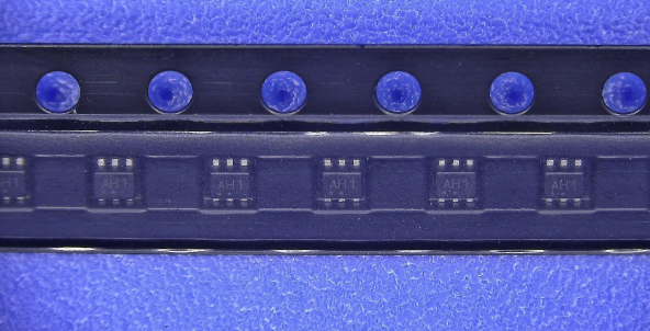
SOT-563 |
| Basic package type |
Lead-Frame SMT |
| Number of pins |
6 |
| Pin shape |
Flat |
| PCB |
6 |
| ears |
N/R |
| Pin spacing (mm) |
0.5 |
| Package length (mm) |
1.6 |
| Package width (mm) |
1.2 |
| Package height (mm) |
0.55 |
| Package diameter (mm) |
N/R |
| Package Overall Length (mm) |
1.6 |
| Package Overall Width (mm) |
1.6 |
| Package Overall Height (mm) |
0.55 |
| Mounting surface height (mm) |
0.55 |
| Install |
Surface Mount |
| Package weight (g) |
not applicable |
| Packaging materials |
Plastic |
| package instruction |
Small Outline Transistor |
| Package series name |
SOT |
| JEDEC |
not applicable |
|
|
MANUFACTURING INFO
|
| Maximum reflow temperature (°C) |
260 |
| Reflow soldering time (seconds) |
30 |
| Number of reflow cycles |
3 |
| standard |
not applicable |
| Reflow temperature source |
Link to datasheet |
| Maximum wave soldering temperature (°C) |
N/R |
| Wave soldering time (seconds) |
N/R |
| Lead Finish(Plating) |
Matte Sn annealed |
| Terminal Base Material |
CuFeNi |
| Number of Wave Cycles |
N/R |
|
|
PACKAGING INFO
|
| Packaging Suffix |
T2 |
| Package |
Tape and reel packaging |
| Packing quantity |
4000 |
| Reel Diameter (in) |
7 |
| Reel Width (mm) |
8.4(Min) |
| Tape Pitch (mm) |
4 |
| Tape Width (mm) |
8 |
| Feed Hole Pitch (mm) |
4 |
| Hole Center to Component Center (mm) |
2 |
| Component Orientation |
Q3 |
| packaging type file |
Link to datasheet |
| Tape Type |
Embossed |
|
|
| APPLICATIONS |
| • Battery Powered Equipments |
| • Portable Communication Equipments |
| • Cameras, Image Sensors and Camcorders |
| |