|
|
• 5.0 V and 3.3 V, ±2% Output Voltage Options
|
• 450 mA Output Current
|
• Very Low Current Consumption
|
• Active Reset Output
|
• Reset Low Down to VQ = 1.0 V
|
• 500 mV (max) Dropout Voltage
|
• Fault Protection
♦ +45 V Peak Transient Voltage
♦ −42 V Reverse Voltage
♦ Short Circuit Protection
♦ Thermal Overload Protection
|
• AEC−Q100 Grade 1 Qualified and PPAP Capable
|
• Pin Compatible with NCV4275
|
• These are Pb−Free Devices
|
|
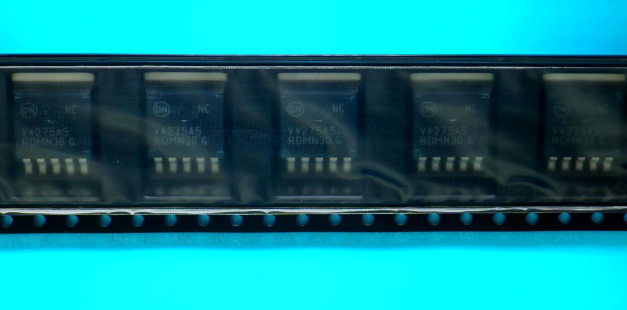
| CATALOG |
| NCV4275ADS50R4G COUNTRY OF ORIGIN |
NCV4275ADS50R4G PARAMETRIC INFO
|
NCV4275ADS50R4G PACKAGE INFO
|
NCV4275ADS50R4G MANUFACTURING INFO
|
NCV4275ADS50R4G PACKAGING INFO
|
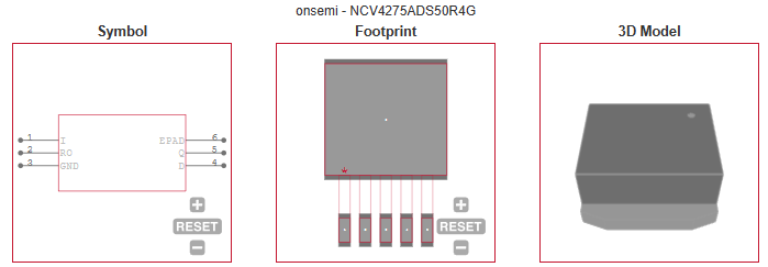
NCV4275ADS50R4G ECAD MODELS
|
NCV4275ADS50R4G APPLICATIONS
|
|
COUNTRY OF ORIGIN
|
Czechia
|
Malaysia
|
|
PARAMETRIC INFO
|
| Type |
LDO |
| Number of Outputs |
1 |
| Maximum Output Current (A) |
0.45 |
| Minimum Operating Temperature (°C) |
-40 |
| Maximum Operating Temperature (°C) |
150 |
| Output Type |
Fixed |
| Output Voltage Range (V) |
1.8 to 10 |
| Regulation Condition Change In Load |
395mA |
| Regulation Condition Change In Line |
24V |
| Junction to Ambient |
74.8°C/W |
| Polarity |
Positive |
| Special Features |
Current Limit|Fault Protection|Short Circuit Protection|Thermal Shutdown Protection |
| Load Regulation |
30mV |
| Line Regulation |
15mV |
| Maximum Quiescent Current (mA) |
0.15 |
| Maximum Dropout Voltage @ Current (V) |
0.5@300mA |
| Minimum Input Voltage (V) |
5.5 |
| Maximum Input Voltage (V) |
42 |
| Output Voltage (V) |
5 |
| Typical Quiescent Current (mA) |
0.14 |
| Typical Dropout Voltage @ Current (V) |
0.25@300mA |
| Accuracy (%) |
±2 |
| Supplier Temperature Grade |
Automotive |
| Minimum Storage Temperature (°C) |
-55 |
| Maximum Storage Temperature (°C) |
150 |
| Typical PSRR (dB) |
60 |
| Output Capacitor Type |
Ceramic |
|
|
PACKAGE INFO
|
| Supplier Package |
D2PAK |
| Basic Package Type |
Lead-Frame SMT |
| Pin Count |
6 |
| Lead Shape |
Gull-wing |
| PCB |
5 |
| Tab |
Tab |
| Pin Pitch (mm) |
1.7 |
| Package Length (mm) |
10.24(Max) |
| Package Width (mm) |
9.35(Max) |
| Package Height (mm) |
4.57(Max) |
| Package Diameter (mm) |
N/R |
| Seated Plane Height (mm) |
4.83(Max) |
| Mounting |
Surface Mount |
| Package Weight (g) |
N/A |
| Package Material |
Plastic |
| Package Description |
Double Deca Watt Package |
| Package Family Name |
TO-263 |
| Jedec |
N/A |
|
|
MANUFACTURING INFO
|
| MSL |
1 |
| Maximum Reflow Temperature (°C) |
260 |
| Reflow Solder Time (Sec) |
30 |
| Number of Reflow Cycle |
3 |
| Standard |
N/A |
| Reflow Temp. Source |
Link to Datasheet |
| Maximum Wave Temperature (°C) |
N/R |
| Wave Solder Time (Sec) |
N/R |
| Lead Finish(Plating) |
Matte Sn annealed |
| Under Plating Material |
N/A |
| Terminal Base Material |
Cu Alloy |
| Number of Wave Cycles |
N/R |
|
|
PACKAGING INFO
|
| Packaging Suffix |
R4 |
| Packaging |
Tape and Reel |
| Quantity Of Packaging |
800 |
| Reel Diameter (in) |
13 |
| Reel Width (mm) |
24.4(Min) |
| Tape Pitch (mm) |
16 |
| Tape Width (mm) |
24 |
| Feed Hole Pitch (mm) |
4 |
| Hole Center to Component Center (mm) |
2 |
| Component Orientation |
Tab Opposing Sprocket Hole |
| Packaging Document |
Link to Datasheet |
| Tape Type |
Embossed |
|
|
ECAD MODELS
|
|
|
APPLICATIONS
|
• Auto Body Electronics
|
|