 |
|
| • Output Current up to 500 mA |
| • 2.9% Output Voltage Accuracy |
| • Low Dropout Voltage (230 mV at 500 mA) |
| • Enable Control Pin (NCP5500 / NCV5500) |
| • Reverse Bias Protection |
| • Short Circuit Protection |
| • Thermal Shutdown |
• Wide Operating Temperature Range
- NCV5500 / NCV5501; −40°C to +125°C Ambient Temperature
- NCP5500 / NCP5501; −40°C to +85°C Ambient Temperature |
| • NCV Prefix for Automotive and Other Applications Requiring
Unique Site and Control Change Requirements; AEC−Q100
Qualified and PPAP Capable |
| • Stable with Low Cost Ceramic Capacitors |
| • These are Pb−Free Devices |
|
| CATALOG |
| NCV5500DTADJRKG COUNTRY OF ORIGIN |
| NCV5500DTADJRKG PARAMETRIC INFO |
| NCV5500DTADJRKG PACKAGE INFO |
| NCV5500DTADJRKG MANUFACTURING INFO |
| NCV5500DTADJRKG PACKAGING INFO |
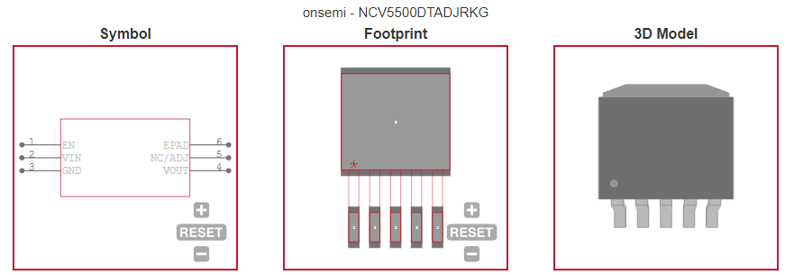
| NCV5500DTADJRKG ECAD MODELS |
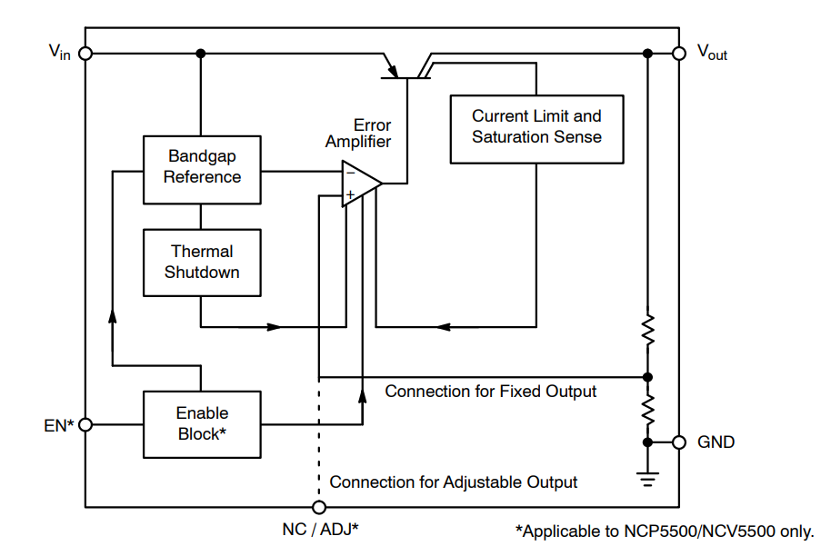
| NCV5500DTADJRKG FUNCTONAL BLOCK DIAGRAM |
| NCV5500DTADJRKG APPLICATIONS |
|
| COUNTRY OF ORIGIN |
| Czechia |
| Malaysia |
|
| PARAMETRIC INFO |
| Type |
LDO |
| Number of Outputs |
1 |
| Maximum Output Current (A) |
0.5 |
| Minimum Operating Temperature (°C) |
-40 |
| Maximum Operating Temperature (°C) |
125 |
| Output Type |
Adjustable |
| Output Voltage Range (V) |
<1.8|1.8 to 10 |
| Junction to Ambient |
60°C/W |
| Junction to Case |
5.2°C/W |
| Polarity |
Positive |
| Special Features |
Enable Control|Short Circuit Protection|Thermal Shutdown Protection |
| Load Regulation |
0.35%(Typ) |
| Line Regulation |
0.1%(Typ) |
| Maximum Dropout Voltage @ Current (V) |
0.09@1mA|0.7@500mA |
| Minimum Input Voltage (V) |
2.5 |
| Maximum Input Voltage (V) |
16 |
| Output Voltage (V) |
1.25 to 5 |
| Typical Dropout Voltage @ Current (V) |
0.005@1mA|0.23@500mA |
| Accuracy (%) |
±2.9 |
| Supplier Temperature Grade |
Automotive |
|
| PACKAGE INFO |
| Supplier Package |
DPAK |
| Basic Package Type |
Lead-Frame SMT |
| Pin Count |
5 |
| Lead Shape |
Gull-wing |
| PCB |
4 |
| Tab |
Tab |
| Pin Pitch (mm) |
1.14 |
| Package Length (mm) |
6.73(Max) |
| Package Width (mm) |
6.22(Max) |
| Package Height (mm) |
2.38(Max) |
| Package Diameter (mm) |
N/R |
| Seated Plane Height (mm) |
2.38(Max) |
| Mounting |
Surface Mount |
| Package Weight (g) |
N/A |
| Package Material |
Plastic |
| Package Description |
Deca Watt Package |
| Package Family Name |
TO-252 |
| Jedec |
N/A |
|
| MANUFACTURING INFO |
| MSL |
1 |
| Maximum Reflow Temperature (°C) |
260 |
| Reflow Solder Time (Sec) |
20 to 40 |
| Number of Reflow Cycle |
3 |
| Standard |
J-STD-020C |
| Reflow Temp. Source |
Link to Datasheet |
| Maximum Wave Temperature (°C) |
N/R |
| Wave Solder Time (Sec) |
N/R |
| Lead Finish(Plating) |
Matte Sn annealed |
| Under Plating Material |
N/A |
| Terminal Base Material |
CuNi |
|
| PACKAGING INFO |
| Packaging Suffix |
RK |
| Packaging |
Tape and Reel |
| Quantity Of Packaging |
2500 |
| Packaging Document |
Link to Datasheet |
|
| ECAD MODELS |
 |
|
| FUNCTONAL BLOCK DIAGRAM |
 |
|
| APPLICATIONS |
| • Automotive |
| • Industrial and Consumer |
| • Post SMPS Regulation |
| • Point of Use Regulation |
|