|
|
• Designed for 1.65 V to 5.5 V VCC Operation
|
• Input Overvoltage Tolerant up to 5.5 V
|
• IOFF Supports Partial Power Down Protection
|
• Sink 24 mA at 3.0 V
|
• Available in SC−88, SC−74 and UDFN6 Packages
|
• Chip Complexity < 100 FETs
|
• NLV Prefix for Automotive and Other Applications RequiringUnique Site and Control Change Requirements; AEC−Q100Qualified and PPAP Capable
|
• These Devices are Pb−Free, Halogen Free/BFR Free and are RoHSCompliant
|
|
| CATALOG |
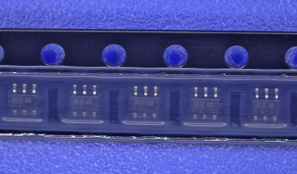
NL27WZU04DFT2G Country of Origin
|
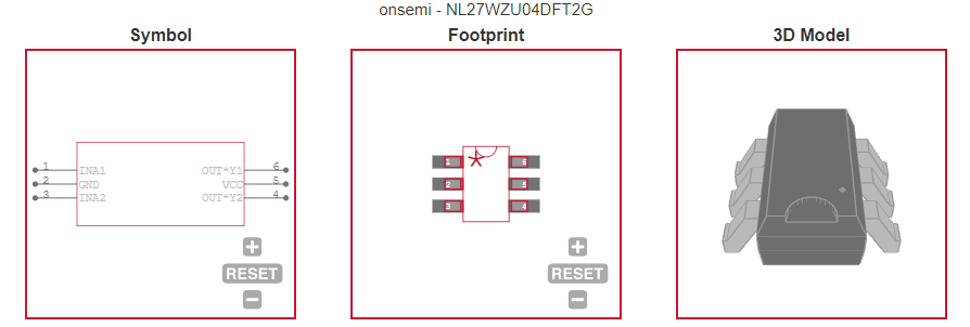
NL27WZU04DFT2G Parametric Info
|
NL27WZU04DFT2G Package Info
|
NL27WZU04DFT2G Manufacturing Info
|
NL27WZU04DFT2G Packaging Info
|
NL27WZU04DFT2G ECAD Models
|
|
COUNTRY OF ORIGIN
|
Malaysia
|
China
|
|
PARAMETRIC INFO
|
| Logic Family |
LCX |
| Process Technology |
CMOS |
| Logic Function |
Inverter |
| Number of Elements per Chip |
2 |
| Minimum Operating Supply Voltage (V) |
1.65 |
| Maximum Operating Supply Voltage (V) |
5.5 |
| Typical Operating Supply Voltage (V) |
1.8|2.5|3.3|5 |
| Minimum Operating Temperature (°C) |
-40 |
| Maximum Operating Temperature (°C) |
125 |
| Maximum Propagation Delay Time @ Maximum CL (ns) |
6.4@3.3V|5.6@5V|1.8@1.8V |
| Absolute Propagation Delay Time (ns) |
11 |
| Propagation Delay Test Condition (pF) |
50 |
| Maximum High Level Output Current (mA) |
-16 |
| Maximum Low Level Output Current (mA) |
16 |
| Maximum Quiescent Current (uA) |
1 |
|
|
PACKAGE INFO
|
| Supplier Package |
SC-88 |
| Basic Package Type |
Lead-Frame SMT |
| Pin Count |
6 |
| PCB |
6 |
| Tab |
N/R |
| Pin Pitch (mm) |
0.65 |
| Package Length (mm) |
2 |
| Package Width (mm) |
1.25 |
| Package Height (mm) |
0.9 |
| Package Diameter (mm) |
N/R |
| Package Overall Length (mm) |
2 |
| Package Overall Width (mm) |
2.1 |
| Package Overall Height (mm) |
1.1(Max) |
| Seated Plane Height (mm) |
1.1(Max) |
| Mounting |
Surface Mount |
| Package Weight (g) |
N/A |
| Package Material |
Plastic |
| Package Family Name |
SOT |
| Jedec |
N/A |
|
|
MANUFACTURING INFO
|
| MSL |
1 |
| Maximum Reflow Temperature (°C) |
260 |
| Reflow Solder Time (Sec) |
20 to 40 |
| Number of Reflow Cycle |
3 |
| Standard |
J-STD-020C |
| Reflow Temp. Source |
Link to Datasheet |
| Maximum Wave Temperature (°C) |
N/R |
| Wave Solder Time (Sec) |
N/R |
| Lead Finish(Plating) |
Matte Sn annealed |
| Under Plating Material |
N/A |
| Terminal Base Material |
CuFeNi |
|
|
PACKAGING INFO
|
| Packaging Suffix |
T2 |
| Packaging |
Tape and Reel |
| Quantity Of Packaging |
3000 |
| Packaging Document |
Link to Datasheet |
|
|
ECAD MODELS
|
|
|
|