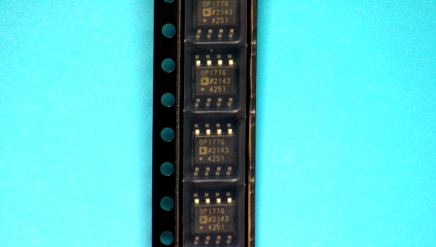
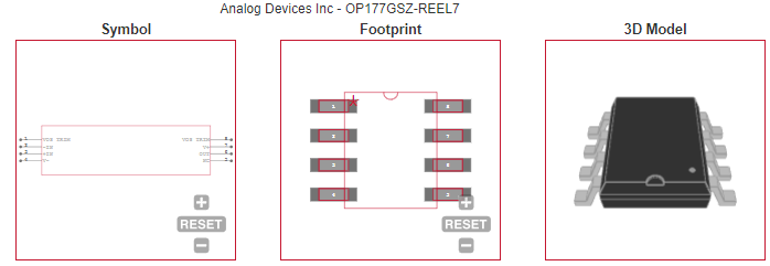
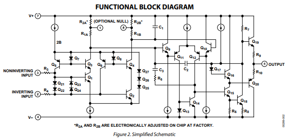
OP177GSZ-REEL7 Analog Devices IC OPAMP GP 600KHZ 8SOIC

label:
2024/02/19 381


• Ultralow offset voltage TA = 25°C, 25 μV maximum
• Outstanding offset voltage drift 0.3 μV/°C maximum
• Excellent open-loop gain and gain linearity 12 V/μV typical
• CMRR: 130 dB minimum
• PSRR: 115 dB minimum
• Low supply current 2.0 mA maximum
• Fits industry-standard precision operational amplifier sockets


CATALOG
OP177GSZ-REEL7 COUNTRY OF ORIGIN
OP177GSZ-REEL7 PARAMETRIC INFO
OP177GSZ-REEL7 PACKAGE INFO
OP177GSZ-REEL7 MANUFACTURING INFO
OP177GSZ-REEL7 PACKAGING INFO
OP177GSZ-REEL7 ECAD MODELS
OP177GSZ-REEL7 FUNCTIONAL BLOCK DIAGRAM


COUNTRY OF ORIGIN
China


PARAMETRIC INFO
Manufacturer Type Precision Amplifier
type Precision Amplifier
Number of Channels per Chip 1
Process Technology Bipolar
Minimum PSRR (dB) 110
Maximum Quiescent Current (mA) 2@±15V
Minimum Dual Supply Voltage (V) ±3
Typical Gain Bandwidth Product (MHz) 0.6
Maximum Input Offset Voltage (mV) 0.06@±15V
Typical Dual Supply Voltage (V) ±5|±9|±12|±15
Maximum Input Offset Current (uA) 0.0028@±15V
Maximum Dual Supply Voltage (V) ±18
Maximum Input Voltage Range (V) ±14
Maximum Operating Supply Voltage (V) ±18
Maximum Input Bias Current (uA) 0.0028@±15V
Minimum CMRR (dB) 115
Maximum Supply Voltage Range (V) 36 to 37
Minimum CMRR Range (dB) >=115
Typical Voltage Gain (dB) 135.56
Typical Slew Rate (V/us) 0.3@±15V
Minimum Slew Rate (V/us) 0.1@±15V
Typical Input Offset Current (uA) 0.0003@±15V
Typical Input Bias Current (uA) 0.0012@±15V
Shut Down Support no
Minimum Operating Temperature (°C) -40
Maximum Operating Temperature (°C) 85
Supplier Temperature Rating Extended Industrial
Minimum Storage Temperature (°C) -65
Maximum Storage Temperature (°C) 125
Power Supply Type Dual
Maximum Power Dissipation (mW) 500
Typical Output Resistance (Ohm) 60
Input Offset Voltage Drift (uV/°C) 1.2


PACKAGE INFO
Supplier packaging SOIC N
Basic package type Lead-Frame SMT
Number of pins 8
Pin shape Gull-wing
PCB 8
ears N/R
Pin spacing (mm) 1.27
Package length (mm) 5(Max)
Package width (mm) 4(Max)
Package height (mm) 1.5(Max)
Package diameter (mm) N/R
Package Overall Length (mm) 5(Max)
Package Overall Width (mm) 6.2(Max)
Package Overall Height (mm) 1.75(Max)
Mounting surface height (mm) 1.75(Max)
Install Surface Mount
Package weight (g) not applicable
Packaging materials Plastic
package instruction Small Outline IC Narrow Body
Package series name SO
JEDEC MS-012AA
Package outline Link to datasheet


MANUFACTURING INFO
MSL 1
Maximum reflow temperature (°C) 260
Reflow soldering time (seconds) 30
Number of reflow cycles 3
standard J-STD-020D
Maximum wave soldering temperature (°C) N/R
Wave soldering time (seconds) N/R
Lead Finish(Plating) Matte Sn annealed
Plating materials Ag
Terminal Base Material Cu Alloy
Number of Wave Cycles N/R


ECAD MODELS


FUNCTIONAL BLOCK DIAGRAM


Продукт RFQ