
|
|
• Low offset voltage: 60 μV maximum
|
• Very low offset voltage drift: 0.7 μV/°C maximum
|
• Low input bias current: 2 nA maximum
|
• Low noise: 8 nV/√Hz typical
|
• CMRR, PSRR, and AVO > 120 dB minimum
|
• Low supply current: 400 μA per amplifier
|
• Dual supply operation: ±2.5 V to ±15 V
|
• Unity-gain stable
|
• No phase reversal
|
• Inputs internally protected beyond supply voltage
|
|
| CATALOG |
OP4177ARZ-REEL7 COUNTRY OF ORIGIN
|
OP4177ARZ-REEL7 PARAMETRIC INFO
|
OP4177ARZ-REEL7 PACKAGE INFO
|
OP4177ARZ-REEL7 MANUFACTURING INFO
|
OP4177ARZ-REEL7 PACKAGING INFO
|
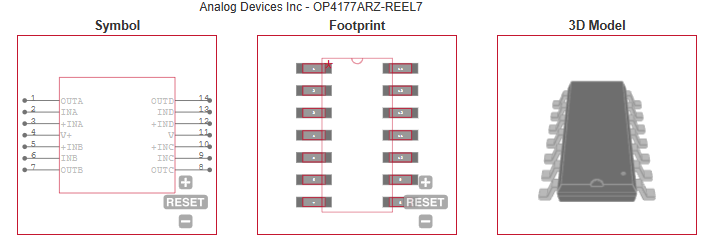
OP4177ARZ-REEL7 ECAD MODELS
|
OP4177ARZ-REEL7 APPLICATIONS
|
|
COUNTRY OF ORIGIN
|
Taiwan (Province of China)
|
Philippines
|
|
PARAMETRIC INFO
|
| Manufacturer Type |
Precision Amplifier |
| Type |
Precision Amplifier |
| Number of Channels per Chip |
4 |
| Minimum PSRR (dB) |
118 |
| Minimum Dual Supply Voltage (V) |
±2.5 |
| Typical Gain Bandwidth Product (MHz) |
1.3 |
| Maximum Input Offset Voltage (mV) |
0.075@±5V |
| Typical Dual Supply Voltage (V) |
±3|±5|±9|±12 |
| Maximum Input Offset Current (uA) |
0.001@±5V@-40C to 125C |
| Maximum Dual Supply Voltage (V) |
±15 |
| Maximum Input Voltage Range (V) |
-3.5 to 3.5 |
| Maximum Operating Supply Voltage (V) |
±15 |
| Maximum Input Bias Current (uA) |
0.002@±5V@-40C to 125C |
| Minimum CMRR (dB) |
120 |
| Maximum Supply Voltage Range (V) |
30 to 32 |
| Minimum CMRR Range (dB) |
>=115 |
| Typical Voltage Gain (dB) |
126.02 |
| Typical Slew Rate (V/us) |
0.7@±5V |
| Typical Output Current (mA) |
10@±5V |
| Typical Input Noise Voltage Density (nV/rtHz) |
7.9@±5V |
| Typical Noninverting Input Current Noise Density (pA/rtHz) |
0.2@±5V |
| Typical Input Bias Current (uA) |
0.0002@±5V@-40C to 125C |
| Shut Down Support |
No |
| Minimum Operating Temperature (°C) |
-40 |
| Maximum Operating Temperature (°C) |
125 |
| Minimum Storage Temperature (°C) |
-65 |
| Maximum Storage Temperature (°C) |
150 |
| Power Supply Type |
Dual |
| Maximum Supply Current (mA) |
2@±5V |
| Typical High Level Output Voltage (V) |
14.1 |
| Typical Low Level Output Voltage (V) |
-14.1 |
| Input Offset Voltage Drift (uV/°C) |
0.9 |
|
|
PACKAGE INFO
|
| Supplier Package |
SOIC N |
| Basic Package Type |
Lead-Frame SMT |
| Pin Count |
14 |
| Lead Shape |
Gull-wing |
| PCB |
14 |
| Tab |
N/R |
| Pin Pitch (mm) |
1.27 |
| Package Length (mm) |
8.75(Max) |
| Package Width (mm) |
4(Max) |
| Package Height (mm) |
1.5(Max) |
| Package Diameter (mm) |
N/R |
| Seated Plane Height (mm) |
1.75(Max) |
| Mounting |
Surface Mount |
| Package Weight (g) |
N/A |
| Package Material |
Plastic |
| Package Description |
Small Outline IC Narrow Body |
| Package Family Name |
SO |
| Jedec |
MS-012AB |
| Package Outline |
Link to Datasheet |
|
|
MANUFACTURING INFO
|
| MSL |
3 |
| Maximum Reflow Temperature (°C) |
260 |
| Reflow Solder Time (Sec) |
30 |
| Number of Reflow Cycle |
3 |
| Standard |
J-STD-020D |
| Maximum Wave Temperature (°C) |
N/R |
| Wave Solder Time (Sec) |
N/R |
| Lead Finish(Plating) |
Matte Sn annealed |
| Under Plating Material |
Ag |
| Terminal Base Material |
Cu Alloy |
| Number of Wave Cycles |
N/R |
|
|
PACKAGING INFO
|
| Packaging Suffix |
REEL7 |
| Packaging |
Tape and Reel |
| Quantity Of Packaging |
1000 |
| Reel Diameter (in) |
7 |
| Tape Pitch (mm) |
8 |
| Tape Width (mm) |
16 |
| Component Orientation |
Q1 |
| Packaging Document |
Link to Datasheet |
| Tape Material |
Plastic |
| Tape Type |
Embossed |
|
|
| ECAD MODELS |
 |
|
| APPLICATIONS |
| • Wireless base station control circuits |
| • Optical network control circuits |
| • Instrumentation |
| • Sensors and controls Thermocouples Resistor thermal detectors (RTDs) Strain bridges Shunt current measurements |
| • Precision filters |
| |