 |
|
| • Very-low offset drift: 1 μV/°C maximum |
| • Very-low offset: 120 μV |
| • Low input bias current: 10 pA maximum |
| • Very-low 1/f noise: 250 nVPP, 0.1 Hz to 10 Hz |
| • Low noise: 5.1 nV/√Hz |
| • Slew rate: 20 V/μs |
| • Low supply current: 2 mA maximum |
| • Input voltage range includes V– supply
|
| • Single-supply operation: 4.5 V to 36 V |
| • Dual-supply operation: ±2.25 V to ±18 V |
| • No phase reversal
|
• Packages:
– Industry-standard SOIC, SON, SOT-23,
TSSOP, and VSSOP |
|
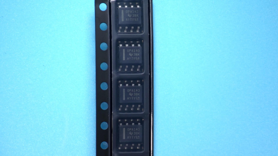
| CATALOG |
| OPA140AID COUNTRY OF ORIGIN |
| OPA140AID PARAMETRIC INFO |
| OPA140AID PACKAGE INFO |
| OPA140AID MANUFACTURING INFO |
| OPA140AID PACKAGING INFO |
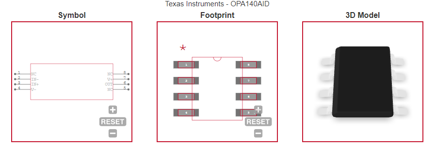
| OPA140AID ECAD MODELS |
| OPA140AID FUNCTIONAL BLOCK DIAGRAM |
| OPA140AID APPLICATIONS
|
|
| COUNTRY OF ORIGIN |
| Malaysia |
|
| PARAMETRIC INFO |
| Manufacturer Type |
Precision Amplifier |
| Type |
Precision Amplifier |
| Rail to Rail |
Rail to Rail Output |
| Minimum Single Supply Voltage (V) |
4.5 |
| Number of Channels per Chip |
1 |
| Minimum PSRR (dB) |
140(Typ) |
| Typical Single Supply Voltage (V) |
5|9|12|15|18|24|28 |
| Maximum Single Supply Voltage (V) |
36 |
| Minimum Dual Supply Voltage (V) |
±2.25 |
| Typical Gain Bandwidth Product (MHz) |
11 |
| Maximum Input Offset Voltage (mV) |
0.12@±18V |
| Typical Dual Supply Voltage (V) |
±3|±5|±9|±12|±15 |
| Maximum Input Offset Current (uA) |
0.00001@±18V |
| Maximum Dual Supply Voltage (V) |
±18 |
| Maximum Operating Supply Voltage (V) |
±18|36 |
| Maximum Input Bias Current (uA) |
0.00001@±18V |
| Minimum CMRR (dB) |
126 |
| Maximum Supply Voltage Range (V) |
36 to 37 |
| Minimum CMRR Range (dB) |
>=115 |
| Typical Voltage Gain (dB) |
126 |
| Typical Slew Rate (V/us) |
20@±18V |
| Typical Input Offset Current (uA) |
0.0000005@±18V |
| Typical Settling Time (ns) |
1600 |
| Typical Output Current (mA) |
30 |
| Typical Input Noise Voltage Density (nV/rtHz) |
8@±18V |
| Typical Noninverting Input Current Noise Density (pA/rtHz) |
0.0008@±18V |
| Shut Down Support |
No |
| Minimum Operating Temperature (°C) |
-40 |
| Maximum Operating Temperature (°C) |
125 |
| Minimum Storage Temperature (°C) |
-65 |
| Maximum Storage Temperature (°C) |
150 |
| Power Supply Type |
Single|Dual |
|
| |
| PACKAGE INFO |
| Supplier Package |
SOIC |
| Basic Package Type |
Lead-Frame SMT |
| Pin Count |
8 |
| Lead Shape |
Gull-wing |
| PCB |
8 |
| Tab |
N/R |
| Pin Pitch (mm) |
1.27 |
| Package Length (mm) |
5(Max) |
| Package Width (mm) |
3.98(Max) |
| Package Height (mm) |
1.5(Max) |
| Package Diameter (mm) |
N/R |
| Package Overall Length (mm) |
5(Max) |
| Package Overall Width (mm) |
6.19(Max) |
| Package Overall Height (mm) |
1.75(Max) |
| Seated Plane Height (mm) |
1.75(Max) |
| Mounting |
Surface Mount |
| Package Weight (g) |
N/A |
| Package Material |
Plastic |
| Package Description |
Small Outline IC |
| Package Family Name |
SO |
| Jedec |
MS-012AA |
| Package Outline |
Link to Datasheet |
|
| |
| MANUFACTURING INFO |
| MSL |
2 |
| Maximum Reflow Temperature (°C) |
260 |
| Reflow Solder Time (Sec) |
30 |
| Number of Reflow Cycle |
3 |
| Standard |
J-STD-020D |
| Reflow Temp. Source |
Link to Datasheet |
| Maximum Wave Temperature (°C) |
N/R |
| Wave Solder Time (Sec) |
N/R |
| Lead Finish(Plating) |
Au |
| Under Plating Material |
Pd over Ni |
| Terminal Base Material |
Cu Alloy |
| Number of Wave Cycles |
N/R |
|
| |
| PACKAGING INFO |
| Packaging |
Tube |
| Quantity Of Packaging |
75 |
| Packaging Document |
Link to Datasheet |
|
| |
| ECAD MODELS |
 |
|
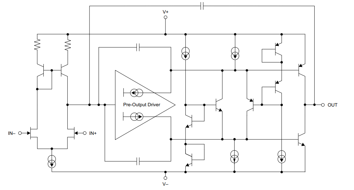
| FUNCTIONAL BLOCK DIAGRAM |
 |
|
| APPLICATIONS
|
| • Intra-dc interconnect (metro) |
| • Semiconductor test |
| • Chemistry and gas analyzer |
| • DC power supply, ac source, electronic load
|
| • Data acquisition (DAQ) |
| • Lab and field instrumentation |
| |
| |