|
|
• Supply range: 2.7 to 36 V, ±1.35 V to ±18 V
|
• Low noise: 14 nV/√Hz
|
• Low offset drift: ±0.3 µV/°C (typical)
|
| • RFI filtered inputs |
| • Input range includes the negative supply |
| • Input range operates to positive supply |
| • Rail-to-rail outpu |
| • Gain bandwidth: 3 MHz |
| • Low quiescent current: 475 µA per amplifier |
| • High common-mode rejection: 120 dB (typical) |
| • Low-input bias current: 8 pA |
| • Industry-standard packages:– 8-pin SOIC– 8-pin MSOP– 14-pin TSSOP |
| • Micro packages:– Single in SOT-553– Dual in VSSOP-8 |
|
| CATALOG |
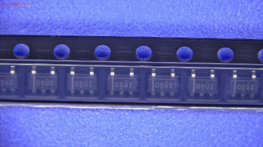
| OPA171AIDBVT COUNTRY OF ORIGIN |
OPA171AIDBVT PARAMETRIC INFO
|
OPA171AIDBVT PACKAGE INFO
|
OPA171AIDBVT MANUFACTURING INFO
|
OPA171AIDBVT PACKAGING INFO
|
OPA171AIDBVT EACD MODELS
|
| OPA171AIDBVT APPLICATIONS |
|
| COUNTRY OF ORIGIN |
| China |
| Philippines |
| Malaysia |
| Thailand |
|
PARAMETRIC INFO
|
| Manufacturer Type |
Precision Amplifier |
| type |
Precision Amplifier |
| Rail to Rail |
Rail to Rail Output |
| Minimum Single Supply Voltage (V) |
2.7 |
| Number of Channels per Chip |
1 |
| Minimum PSRR (dB) |
120(Typ) |
| Typical Single Supply Voltage (V) |
3|5|9|12|15|18|24|28 |
| Maximum Single Supply Voltage (V) |
36 |
| Maximum Quiescent Current (mA) |
0.595@36V |
| Minimum Dual Supply Voltage (V) |
±1.35 |
| Typical Gain Bandwidth Product (MHz) |
3 |
| Maximum Input Offset Voltage (mV) |
1.8@36V |
| Typical Dual Supply Voltage (V) |
±3|±5|±9|±12|±15 |
| Maximum Input Offset Current (uA) |
0.000004(Typ)@36V |
| Maximum Dual Supply Voltage (V) |
±18 |
| Maximum Operating Supply Voltage (V) |
±18|36 |
| Maximum Input Bias Current (uA) |
0.000015@36V |
| Minimum CMRR (dB) |
90 |
| Maximum Supply Voltage Range (V) |
36 to 37 |
| Minimum CMRR Range (dB) |
90 to 95 |
| Typical Voltage Gain (dB) |
130 |
| Typical Slew Rate (V/us) |
1.5@36V |
| Typical Settling Time (ns) |
10000 |
| Typical Output Current (mA) |
35 |
| Typical Input Noise Voltage Density (nV/rtHz) |
25@36V |
| Shut Down Support |
no |
| Minimum Operating Temperature (°C) |
-40 |
| Maximum Operating Temperature (°C) |
125 |
| Minimum Storage Temperature (°C) |
-65 |
| Maximum Storage Temperature (°C) |
150 |
| Power Supply Type |
Single|Dual |
|
|
PACKAGE INFO
|
| Supplier packaging |
SOT-23 |
| Basic package type |
Lead-Frame SMT |
| Number of pins |
5 |
| Pin shape |
Gull-wing |
| PCB |
5 |
| ears |
N/R |
| Pin spacing (mm) |
0.95 |
| Package length (mm) |
3.05(Max) |
| Package width (mm) |
1.75(Max) |
| Package height (mm) |
1.1 |
| Package diameter (mm) |
N/R |
| Package Overall Length (mm) |
3.05(Max) |
| Package Overall Width (mm) |
3(Max) |
| Package Overall Height (mm) |
1.45(Max) |
| Mounting surface height (mm) |
1.45(Max) |
| Install |
Surface Mount |
| Package weight (g) |
not applicable |
| Packaging materials |
Plastic |
| package instruction |
Small Outline Transistor |
| Package series name |
SOT |
| JEDEC |
MO-178AA |
| Package outline |
Link to datasheet |
|
|
MANUFACTURING INFO
|
| MSL |
2 |
| Maximum reflow temperature (°C) |
260 |
| Reflow soldering time (seconds) |
30 |
| Number of reflow cycles |
3 |
| standard |
J-STD-020D |
| Reflow temperature source |
Link to datasheet |
| Maximum wave soldering temperature (°C) |
N/R |
| Wave soldering time (seconds) |
N/R |
| Lead Finish(Plating) |
Au |
| Plating materials |
Pd over Ni |
| Terminal Base Material |
Cu Alloy |
|
|
PACKAGING INFO
|
| Packaging Suffix |
T |
| Package |
Tape and reel packaging |
| Packing quantity |
250 |
| Reel Diameter (in) |
7 |
| Tape Pitch (mm) |
4 |
| Tape Width (mm) |
8 |
| Component Orientation |
Q3 |
| packaging type file |
Link to datasheet |
|
|
ECAD MODELS
|
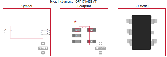
|
|
APPLICATIONS
|
• Tracking amplifier in power modules
|
| • Merchant power supplies |
| • Transducer amplifiers |
| • Bridge amplifiers |
| • Temperature measurement |
| • Strain gauge amplifiers |
| • Precision integrators |
| • Battery-powered instruments |
| • Test equipment |
| |