|
|
• Low Offset Voltage: ±100 µV (maximum)
|
• Low Offset Voltage Drift: ±0.5 µV/°C (typical)
|
• Low Bias Current: ±5 pA (typical)
|
• High Common-Mode Rejection: 140 dB
|
• Low Noise: 15 nV/√Hz at 1 kHz
|
| • Rail-to-Rail Input and Output |
| • Differential Input Voltage Range to Supply Rail |
| • Wide Bandwidth: 2.5-MHz GBW |
| • Low Quiescent Current: 140 µA per Amplifier
(typical) |
| • Wide Supply: ±2.25 V to ±18 V, 4.5 V to 36 V |
| • EMI/RFI Filtered Inputs |
| • High Capacitive Load Drive Capability: 1 nF |
| • Industry Standard Packages:
– Single in SOIC-8, SOT-5, and VSSOP-8
– Dual in SOIC-8 and VSSOP-8
– Quad in SOIC-14, TSSOP-14, and QFN-16 |
|
| CATALOG |
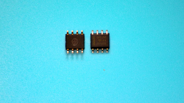
OPA2196ID COUNTRY OF ORIGIN
|
OPA2196ID PARAMETRIC INFO
|
OPA2196ID PACKAGE INFO
|
OPA2196ID MANUFACTURING INFO
|
OPA2196ID PACKAGING INFO
|
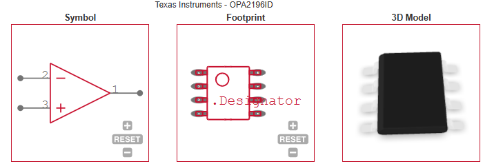
OPA2196ID ECAD MODELS
|
OPA2196ID APPLICATIONS
|
|
COUNTRY OF ORIGIN
|
Malaysia
|
|
PARAMETRIC INFO
|
| Manufacturer Type |
Low Offset Voltage Amplifier |
| Type |
Low Offset Voltage Amplifier |
| Rail to Rail |
Rail to Rail Input/Output |
| Minimum Single Supply Voltage (V) |
4.5 |
| Number of Channels per Chip |
2 |
| Minimum PSRR (dB) |
130.46(Typ) |
| Typical Single Supply Voltage (V) |
5|9|12|15|18|24|28 |
| Typical Input Resistance (Ohm) |
10T |
| Maximum Single Supply Voltage (V) |
36 |
| Maximum Quiescent Current (mA) |
0.4@36V |
| Minimum Dual Supply Voltage (V) |
±2.25 |
| Typical Gain Bandwidth Product (MHz) |
2.5 |
| Maximum Input Offset Voltage (mV) |
0.1@±18V |
| Typical Dual Supply Voltage (V) |
±3|±5|±9|±12|±15 |
| Maximum Input Offset Current (uA) |
0.00002@36V |
| Maximum Dual Supply Voltage (V) |
±18 |
| Maximum Operating Supply Voltage (V) |
±18|36 |
| Maximum Input Bias Current (uA) |
0.00002@36V |
| Minimum CMRR (dB) |
96 |
| Maximum Supply Voltage Range (V) |
36 to 37 |
| Minimum CMRR Range (dB) |
95 to 105 |
| Typical Voltage Gain (dB) |
140 |
| Typical Slew Rate (V/us) |
7.5@±18V |
| Typical Input Offset Current (uA) |
0.000002@36V |
| Typical Settling Time (ns) |
3700 |
| Typical Output Current (mA) |
65 |
| Typical Input Noise Voltage Density (nV/rtHz) |
53@36V |
| Typical Noninverting Input Current Noise Density (pA/rtHz) |
0.0015@36V |
| Typical Input Bias Current (uA) |
0.000005@36V |
| Shut Down Support |
No |
| Minimum Operating Temperature (°C) |
-40 |
| Maximum Operating Temperature (°C) |
125 |
| Minimum Storage Temperature (°C) |
-65 |
| Maximum Storage Temperature (°C) |
150 |
| Power Supply Type |
Single|Dual |
| Typical Output Resistance (Ohm) |
700 |
| Input Offset Voltage Drift (uV/°C) |
±0.8(Typ) |
|
|
PACKAGE INFO
|
| Supplier Package |
SOIC |
| Basic Package Type |
Lead-Frame SMT |
| Pin Count |
8 |
| Lead Shape |
Gull-wing |
| PCB |
8 |
| Tab |
N/R |
| Pin Pitch (mm) |
1.27 |
| Package Length (mm) |
5(Max) |
| Package Width (mm) |
3.98(Max) |
| Package Height (mm) |
1.5(Max) |
| Package Diameter (mm) |
N/R |
| Package Overall Length (mm) |
5(Max) |
| Package Overall Width (mm) |
6.19(Max) |
| Package Overall Height (mm) |
1.75(Max) |
| Seated Plane Height (mm) |
1.75(Max) |
| Mounting |
Surface Mount |
| Package Weight (g) |
N/A |
| Package Material |
Plastic |
| Package Description |
Small Outline IC |
| Package Family Name |
SO |
| Jedec |
MS-012AA |
| Package Outline |
Link to Datasheet |
|
|
MANUFACTURING INFO
|
| MSL |
2 |
| Maximum Reflow Temperature (°C) |
260 |
| Reflow Solder Time (Sec) |
30 |
| Number of Reflow Cycle |
3 |
| Standard |
J-STD-020D |
| Reflow Temp. Source |
Link to Datasheet |
| Maximum Wave Temperature (°C) |
N/R |
| Wave Solder Time (Sec) |
N/R |
| Lead Finish(Plating) |
Au |
| Under Plating Material |
Pd over Ni |
| Terminal Base Material |
Cu Alloy |
|
|
PACKAGING INFO
|
| Packaging |
Tube |
| Quantity Of Packaging |
75 |
|
|
ECAD MODELS
|
|
|
APPLICATIONS
|
• Multiplexed Data-Acquisition Systems
|
| • Test and Measurement Equipment |
• High-Resolution ADC Driver Amplifiers
|
• SAR ADC Reference Buffers
|
• Analog Input and Output Modules
|
| • High-Side and Low-Side Current Sensing |
| • High-Precision Comparator |
| • Medical Instrumentation
|
|
| |