|
|
• Ultra-low offset voltage: 10 μV
|
• Ultra-low drift: ±0.1 μV/°C
|
• High open-loop gain: 134 dB
|
• High common-mode rejection: 140 dB
|
• High power-supply rejection: 130 dB
|
• Low bias current: 1-nA maximum
|
• Wide supply range: ±2 V to ±18 V
|
• Low quiescent current: 800 μA/amplifier
|
• Single, dual, and quad versions
|
• Replaces OP-07, OP-77, and OP-177
|
• For similar performance with ±40-V overvoltage
protection, see the OPA2206
|
|
| CATALOG |
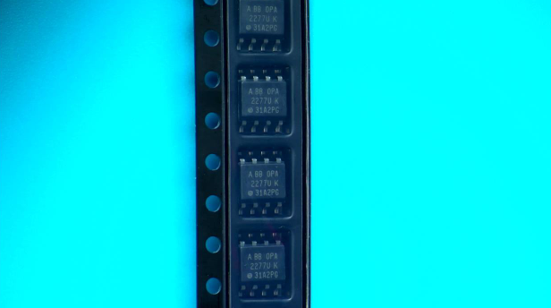
OPA2277UA COUNTRY OF ORIGIN
|
OPA2277UA PARAMETRIC INFO
|
OPA2277UA PACKAGE INFO
|
OPA2277UA MANUFACTURING INFO
|
OPA2277UA PACKAGING INFO
|
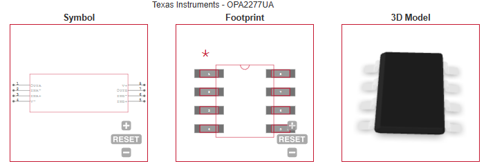
OPA2277UA ECAD MODELS
|
OPA2277UA APPLICATIONS
|
|
COUNTRY OF ORIGIN
|
China
|
Philippines
|
Malaysia
|
Taiwan (Province of China)
|
Thailand
|
United States of America
|
|
PARAMETRIC INFO
|
| Manufacturer Type |
Precision Amplifier |
| Type |
Precision Amplifier |
| Minimum Single Supply Voltage (V) |
4 |
| Number of Channels per Chip |
2 |
| Minimum PSRR (dB) |
130.46(Typ) |
| Typical Single Supply Voltage (V) |
30 |
| Typical Input Resistance (Ohm) |
250G |
| Maximum Single Supply Voltage (V) |
36 |
| Maximum Quiescent Current (mA) |
1.65@30V |
| Minimum Dual Supply Voltage (V) |
±2 |
| Typical Gain Bandwidth Product (MHz) |
1 |
| Maximum Input Offset Voltage (mV) |
0.05@30V |
| Typical Dual Supply Voltage (V) |
±15 |
| Maximum Input Offset Current (uA) |
0.0028@30V |
| Maximum Dual Supply Voltage (V) |
±18 |
| Maximum Operating Supply Voltage (V) |
±18|36 |
| Maximum Input Bias Current (uA) |
0.0028@30V |
| Minimum CMRR (dB) |
115 |
| Maximum Supply Voltage Range (V) |
36 to 37 |
| Minimum CMRR Range (dB) |
>=115 |
| Typical Voltage Gain (dB) |
140 |
| Typical Slew Rate (V/us) |
0.8@30V |
| Typical Input Offset Current (uA) |
0.0005@30V |
| Typical Settling Time (ns) |
16000 |
| Typical Output Current (mA) |
35 |
| Typical Input Noise Voltage Density (nV/rtHz) |
12@30V |
| Typical Noninverting Input Current Noise Density (pA/rtHz) |
0.2@30V |
| Shut Down Support |
No |
| Minimum Operating Temperature (°C) |
-40 |
| Maximum Operating Temperature (°C) |
85 |
| Power Supply Type |
Single|Dual |
| Typical Output Resistance (Ohm) |
40 |
|
|
PACKAGE INFO
|
| Supplier Package |
SOIC |
| Basic Package Type |
Lead-Frame SMT |
| Pin Count |
8 |
| Lead Shape |
Gull-wing |
| PCB |
8 |
| Tab |
N/R |
| Pin Pitch (mm) |
1.27 |
| Package Length (mm) |
5(Max) |
| Package Width (mm) |
3.98(Max) |
| Package Height (mm) |
1.5(Max) |
| Package Diameter (mm) |
N/R |
| Package Overall Length (mm) |
5(Max) |
| Package Overall Width (mm) |
6.19(Max) |
| Package Overall Height (mm) |
1.75(Max) |
| Seated Plane Height (mm) |
1.75(Max) |
| Mounting |
Surface Mount |
| Package Weight (g) |
N/A |
| Package Material |
Plastic |
| Package Description |
Small Outline IC |
| Package Family Name |
SO |
| Jedec |
MS-012AA |
| Package Outline |
Link to Datasheet |
|
|
MANUFACTURING INFO
|
| MSL |
2 |
| Maximum Reflow Temperature (°C) |
260 |
| Reflow Solder Time (Sec) |
30 |
| Number of Reflow Cycle |
3 |
| Standard |
J-STD-020D |
| Reflow Temp. Source |
Link to Datasheet |
| Maximum Wave Temperature (°C) |
N/R |
| Wave Solder Time (Sec) |
N/R |
| Lead Finish(Plating) |
Au |
| Under Plating Material |
Pd over Ni |
| Terminal Base Material |
Cu Alloy |
| Number of Wave Cycles |
N/R |
|
|
PACKAGING INFO
|
| Packaging |
Tube |
| Quantity Of Packaging |
75 |
|
|
ECAD MODELS
|
|
|
APPLICATIONS
|
• Analog input module
|
| • Weigh scale |
• Temperature transmitter
|
• Pressure transmitter
|
| • Data acquisition (DAQ) |
| • Lab and field instrumentation |
• Battery test
|
| |