OPA320SAIDBVR Texas Instruments OPAx320x Precision, 20-MHz, 0.9-pA, Low-Noise, RRIO, CMOS Operational Amplifier With Shutdown

label:
2024/08/6 161
OPA320SAIDBVR Texas Instruments OPAx320x Precision, 20-MHz, 0.9-pA, Low-Noise, RRIO, CMOS Operational Amplifier With Shutdown


• Precision with Zero-Crossover Distortion:– Low Offset Voltage: 150 µV (Maximum)– High CMRR: 114 dB– Rail-to-Rail I/O
• Low Input Bias Current: 0.9 pA (Maximum)
• Low Noise: 7 nV/√Hz at 10 kHz
• Wide Bandwidth: 20 MHz
• Slew Rate: 10 V/µs
• Quiescent Current: 1.45 mA/Ch
• Single-Supply Voltage Range: 1.8 V to 5.5 V
• OPA320S and OPA2320S:– IQ in Shutdown Mode: 0.1 µA
• Unity-Gain Stable
• Small Packages:– SOT-23, VSSOP, SON, and SOIC


CATALOG
OPA320SAIDBVR COUNTRY OF ORIGIN
OPA320SAIDBVR PARAMETRIC INFO
OPA320SAIDBVR PACKAGE INFO
OPA320SAIDBVR MANUFACTURING INFO
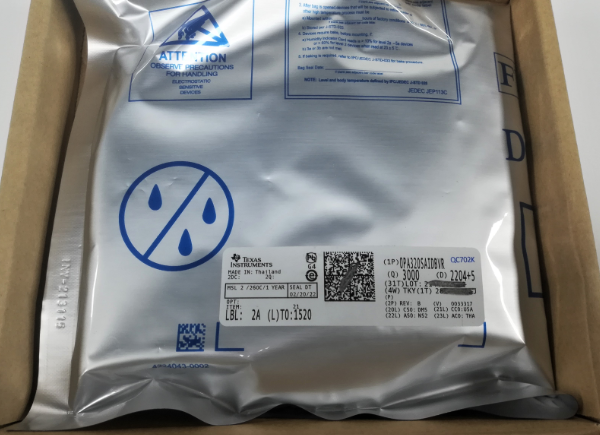
OPA320SAIDBVR PACKAGING INFO
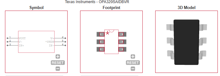
OPA320SAIDBVR ECAD MODELS
OPA320SAIDBVR APPLICATIONS


COUNTRY OF ORIGIN
China
Thailand
Philippines


PARAMETRIC INFO
Manufacturer Type Precision Amplifier
Type Precision Amplifier
Rail to Rail Rail to Rail Input/Output
Minimum Single Supply Voltage (V) 1.8
Number of Channels per Chip 1
Process Technology CMOS
Minimum PSRR (dB) 106(Typ)
Typical Single Supply Voltage (V) 3|5
Maximum Single Supply Voltage (V) 5.5
Output Type CMOS
Maximum Quiescent Current (mA) 1.75@5.5V
Minimum Dual Supply Voltage (V) ±0.9
Typical Gain Bandwidth Product (MHz) 20
Maximum Input Offset Voltage (mV) 0.15@5.5V
Maximum Input Offset Current (uA) 0.0000009@5.5V
Maximum Dual Supply Voltage (V) ±2.75
Maximum Operating Supply Voltage (V) ±2.75|5.5
Maximum Input Bias Current (uA) 0.0000009@5.5V
Minimum CMRR (dB) 100
Maximum Supply Voltage Range (V) 5.5 to 6
Minimum CMRR Range (dB) 95 to 105
Typical Voltage Gain (dB) 132
Typical Slew Rate (V/us) 10@5.5V
Typical Input Offset Current (uA) 0.0000002@5.5V
Typical Settling Time (ns) 500
Typical Output Current (mA) 65
Typical Input Noise Voltage Density (nV/rtHz) 8.5@5.5V
Typical Noninverting Input Current Noise Density (pA/rtHz) 0.0006@5.5V
Typical Input Bias Current (uA) 0.0000002@5.5V
Shut Down Support Yes
Minimum Operating Temperature (°C) -40
Maximum Operating Temperature (°C) 125
Supplier Temperature Grade Extended
Minimum Storage Temperature (°C) -65
Maximum Storage Temperature (°C) 150
Power Supply Type Single|Dual
Typical Output Resistance (Ohm) 90
Input Offset Voltage Drift (uV/°C) 1.5


PACKAGE INFO
Supplier Package SOT-23
Basic Package Type Lead-Frame SMT
Pin Count 6
Lead Shape Gull-wing
PCB 6
Tab N/R
Pin Pitch (mm) 0.95
Package Length (mm) 3.05(Max)
Package Width (mm) 1.75(Max)
Package Height (mm) 1.1
Package Diameter (mm) N/R
Package Overall Length (mm) 3.05(Max)
Package Overall Width (mm) 3(Max)
Package Overall Height (mm) 1.45(Max)
Seated Plane Height (mm) 1.45(Max)
Mounting Surface Mount
Package Weight (g) N/A
Package Material Plastic
Package Description Small Outline Transistor
Package Family Name SOT
Jedec MO-178AB
Package Outline Link to Datasheet


MANUFACTURING INFO
MSL 2
Maximum Reflow Temperature (°C) 260
Reflow Solder Time (Sec) 30
Number of Reflow Cycle 3
Standard J-STD-020D
Reflow Temp. Source Link to Datasheet
Maximum Wave Temperature (°C) 260
Wave Solder Time (Sec) 4
Wave Temp. Source Link to Datasheet
Lead Finish(Plating) Au
Under Plating Material Pd over Ni
Terminal Base Material Cu Alloy
Number of Wave Cycles N/A


PACKAGING INFO
Packaging Suffix DBVR
Packaging Tape and Reel
Quantity Of Packaging 3000
Reel Diameter (in) 7
Tape Pitch (mm) 4
Tape Width (mm) 8
Component Orientation Q3
Packaging Document Link to Datasheet
Tape Type Embossed


ECAD MODELS


APPLICATIONS
• High-Z Sensor Signal Conditioning
• Transimpedance Amplifiers
• Test and Measurement Equipment
• Programmable Logic Controllers (PLCs)
• Motor Control Loops
• Communications
• Input/Output ADC/DAC Buffers
• Active Filters
Продукт RFQ