 |
|
• AEC-Q100 qualified for automotive applications:
– Temperature grade 1: –40°C to +125°C, TA |
| • Low offset voltage: 10 μV (maximum)
|
| • 0.01-Hz to 10-Hz noise: 1.1 μVPP |
| • Quiescent current: 17 μA |
| • Single-supply operation |
| • Supply voltage: 1.8 V to 5.5 V |
| • Rail-to-rail input and output |
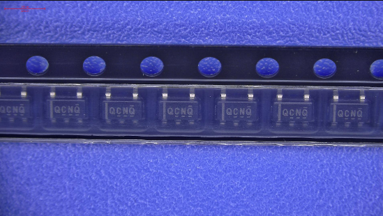
| • Microsize 5-pin SOT-23 (DBV) package |
|
| CATALOG |
| OPA333AQDBVRQ1 COUNTRY OF ORIGIN |
| OPA333AQDBVRQ1 PARAMETRIC INFO |
| OPA333AQDBVRQ1 PACKAGE INFO |
| OPA333AQDBVRQ1 MANUFACTURING INFO |
| OPA333AQDBVRQ1 PACKAGING INFO |
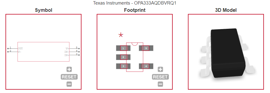
| OPA333AQDBVRQ1 ECAD MODELS |
| OPA333AQDBVRQ1 FUNCTIONAL BLOCK DIAGRAM |
| OPA333AQDBVRQ1 APPLICATIONS
|
|
| COUNTRY OF ORIGIN |
| Thailand |
|
| PARAMETRIC INFO |
| Manufacturer Type |
Micropower Amplifier |
| Type |
Micropower Amplifier |
| Rail to Rail |
Rail to Rail Input/Output |
| Minimum Single Supply Voltage (V) |
1.8 |
| Number of Channels per Chip |
1 |
| Process Technology |
CMOS |
| Minimum PSRR (dB) |
120(Typ) |
| Typical Single Supply Voltage (V) |
3|5 |
| Maximum Single Supply Voltage (V) |
5.5 |
| Output Type |
CMOS |
| Maximum Quiescent Current (mA) |
0.025@5.5V |
| Minimum Dual Supply Voltage (V) |
±0.9 |
| Typical Gain Bandwidth Product (MHz) |
0.35 |
| Maximum Input Offset Voltage (mV) |
0.01@5V |
| Maximum Input Offset Current (uA) |
0.0004@5V |
| Maximum Dual Supply Voltage (V) |
±2.75 |
| Maximum Operating Supply Voltage (V) |
±2.75|5.5 |
| Maximum Input Bias Current (uA) |
0.0002@5V |
| Minimum CMRR (dB) |
106 |
| Maximum Supply Voltage Range (V) |
5.5 to 6 |
| Minimum CMRR Range (dB) |
105 to 115 |
| Typical Voltage Gain (dB) |
130 |
| Typical Slew Rate (V/us) |
0.16@5.5V |
| Typical Noninverting Input Current Noise Density (pA/rtHz) |
0.1@5.5V |
| Typical Input Bias Current (uA) |
0.00007@5V |
| Shut Down Support |
No |
| Minimum Operating Temperature (°C) |
-40 |
| Maximum Operating Temperature (°C) |
125 |
| Supplier Temperature Grade |
Automotive |
| Minimum Storage Temperature (°C) |
-65 |
| Maximum Storage Temperature (°C) |
150 |
| Power Supply Type |
Single|Dual |
|
| |
| PACKAGE INFO |
| Supplier Package |
SOT-23 |
| Basic Package Type |
Lead-Frame SMT |
| Pin Count |
5 |
| Lead Shape |
Gull-wing |
| PCB |
5 |
| Tab |
N/R |
| Pin Pitch (mm) |
0.95 |
| Package Length (mm) |
3.05(Max) |
| Package Width (mm) |
1.75(Max) |
| Package Height (mm) |
1.1 |
| Package Diameter (mm) |
N/R |
| Package Overall Length (mm) |
3.05(Max) |
| Package Overall Width (mm) |
3(Max) |
| Package Overall Height (mm) |
1.45(Max) |
| Seated Plane Height (mm) |
1.45(Max) |
| Mounting |
Surface Mount |
| Package Weight (g) |
N/A |
| Package Material |
Plastic |
| Package Description |
Small Outline Transistor |
| Package Family Name |
SOT |
| Jedec |
MO-178AA |
| Package Outline |
Link to Datasheet |
|
| |
| MANUFACTURING INFO |
| MSL |
1 |
| Maximum Reflow Temperature (°C) |
260 |
| Reflow Solder Time (Sec) |
30 |
| Number of Reflow Cycle |
3 |
| Standard |
J-STD-020D |
| Reflow Temp. Source |
Link to Datasheet |
| Maximum Wave Temperature (°C) |
N/R |
| Wave Solder Time (Sec) |
N/R |
| Lead Finish(Plating) |
Au |
| Under Plating Material |
Pd over Ni |
| Terminal Base Material |
Cu Alloy |
|
| |
| PACKAGING INFO |
| Packaging Suffix |
R |
| Packaging |
Tape and Reel |
| Quantity Of Packaging |
3000 |
| Reel Diameter (in) |
7 |
| Tape Pitch (mm) |
4 |
| Tape Width (mm) |
8 |
| Component Orientation |
Q3 |
| Packaging Document |
Link to Datasheet |
|
| |
| ECAD MODELS |
 |
|
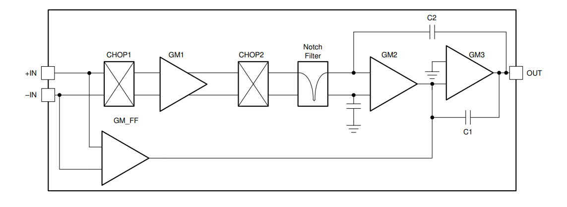
| FUNCTIONAL BLOCK DIAGRAM |
 |
|
| APPLICATIONS |
| • Pump |
| • Position sensor |
| • Vehicle occupant detection sensor |
| • Brake system
|
| • Airbag
|
|