 |
||||||||||||||||||||||||||||||||||||||||||||||||||||||||||||||||||||||||
| |
||||||||||||||||||||||||||||||||||||||||||||||||||||||||||||||||||||||||
| • Gain bandwidth: 50 MHz | ||||||||||||||||||||||||||||||||||||||||||||||||||||||||||||||||||||||||
| • Zerø-crossover distortion topology: – Excellent THD+N: 0.0004% – CMRR: 100 dB (minimum) – Rail-to-rail input and output • Input 100 mV beyond supply rail |
||||||||||||||||||||||||||||||||||||||||||||||||||||||||||||||||||||||||
| • Low noise: 4.5 nV/√Hz at 100 kHz | ||||||||||||||||||||||||||||||||||||||||||||||||||||||||||||||||||||||||
| • Slew rate: 25 V/µs | ||||||||||||||||||||||||||||||||||||||||||||||||||||||||||||||||||||||||
| • Fast settling: 0.3 μs to 0.01% | ||||||||||||||||||||||||||||||||||||||||||||||||||||||||||||||||||||||||
| • Precision: – Low offset: 100 µV – Low input bias current: 0.2 pA |
||||||||||||||||||||||||||||||||||||||||||||||||||||||||||||||||||||||||
| • 2.2-V to 5.5-V operation | ||||||||||||||||||||||||||||||||||||||||||||||||||||||||||||||||||||||||
| |
||||||||||||||||||||||||||||||||||||||||||||||||||||||||||||||||||||||||
| CATALOG | ||||||||||||||||||||||||||||||||||||||||||||||||||||||||||||||||||||||||
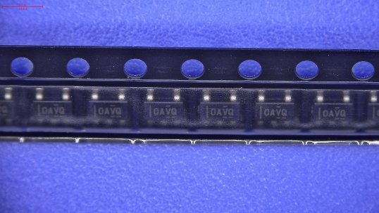
| OPA365AIDBVR COUNTRY OF ORIGIN | ||||||||||||||||||||||||||||||||||||||||||||||||||||||||||||||||||||||||
| OPA365AIDBVR PARAMETRIC INFO | ||||||||||||||||||||||||||||||||||||||||||||||||||||||||||||||||||||||||
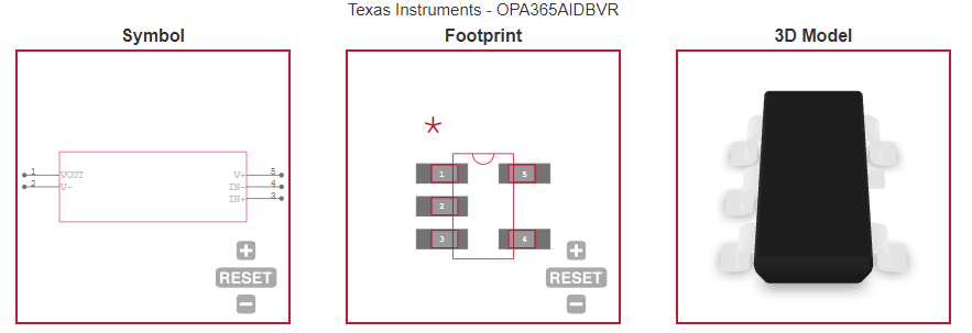
| OPA365AIDBVR PACKAGE INFO | ||||||||||||||||||||||||||||||||||||||||||||||||||||||||||||||||||||||||
| OPA365AIDBVR MANUFACTURING INFO | ||||||||||||||||||||||||||||||||||||||||||||||||||||||||||||||||||||||||
| OPA365AIDBVR PACKAGING INFO | ||||||||||||||||||||||||||||||||||||||||||||||||||||||||||||||||||||||||
| OPA365AIDBVR ECAD MODELS | ||||||||||||||||||||||||||||||||||||||||||||||||||||||||||||||||||||||||
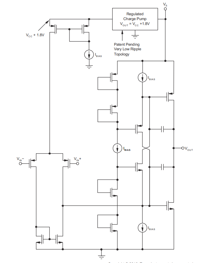
| OPA365AIDBVR FUNCTIONAL BLOCK DIAGRAM | ||||||||||||||||||||||||||||||||||||||||||||||||||||||||||||||||||||||||
| OPA365AIDBVR APPLICATIONS | ||||||||||||||||||||||||||||||||||||||||||||||||||||||||||||||||||||||||
| |
||||||||||||||||||||||||||||||||||||||||||||||||||||||||||||||||||||||||
| COUNTRY OF ORIGIN | ||||||||||||||||||||||||||||||||||||||||||||||||||||||||||||||||||||||||
| China | ||||||||||||||||||||||||||||||||||||||||||||||||||||||||||||||||||||||||
| Thailand | ||||||||||||||||||||||||||||||||||||||||||||||||||||||||||||||||||||||||
| Philippines | ||||||||||||||||||||||||||||||||||||||||||||||||||||||||||||||||||||||||
| Malaysia | ||||||||||||||||||||||||||||||||||||||||||||||||||||||||||||||||||||||||
| |
||||||||||||||||||||||||||||||||||||||||||||||||||||||||||||||||||||||||
| PARAMETRIC INFO | ||||||||||||||||||||||||||||||||||||||||||||||||||||||||||||||||||||||||
|
||||||||||||||||||||||||||||||||||||||||||||||||||||||||||||||||||||||||
| PACKAGE INFO | ||||||||||||||||||||||||||||||||||||||||||||||||||||||||||||||||||||||||
|
||||||||||||||||||||||||||||||||||||||||||||||||||||||||||||||||||||||||
| MANUFACTURING INFO | ||||||||||||||||||||||||||||||||||||||||||||||||||||||||||||||||||||||||
|
||||||||||||||||||||||||||||||||||||||||||||||||||||||||||||||||||||||||
| PACKAGING INFO | ||||||||||||||||||||||||||||||||||||||||||||||||||||||||||||||||||||||||
|
||||||||||||||||||||||||||||||||||||||||||||||||||||||||||||||||||||||||
| ECAD MODELS | ||||||||||||||||||||||||||||||||||||||||||||||||||||||||||||||||||||||||
 |
||||||||||||||||||||||||||||||||||||||||||||||||||||||||||||||||||||||||
| |
||||||||||||||||||||||||||||||||||||||||||||||||||||||||||||||||||||||||
| FUNCTIONAL BLOCK DIAGRAM | ||||||||||||||||||||||||||||||||||||||||||||||||||||||||||||||||||||||||
 |
||||||||||||||||||||||||||||||||||||||||||||||||||||||||||||||||||||||||
| |
||||||||||||||||||||||||||||||||||||||||||||||||||||||||||||||||||||||||
| APPLICATIONS | ||||||||||||||||||||||||||||||||||||||||||||||||||||||||||||||||||||||||
| • Signal conditioning | ||||||||||||||||||||||||||||||||||||||||||||||||||||||||||||||||||||||||
| • Data acquisition | ||||||||||||||||||||||||||||||||||||||||||||||||||||||||||||||||||||||||
| • Process control | ||||||||||||||||||||||||||||||||||||||||||||||||||||||||||||||||||||||||
| • Active filters | ||||||||||||||||||||||||||||||||||||||||||||||||||||||||||||||||||||||||
| • Test equipment | ||||||||||||||||||||||||||||||||||||||||||||||||||||||||||||||||||||||||
| • Audio | ||||||||||||||||||||||||||||||||||||||||||||||||||||||||||||||||||||||||
| • Wideband amplifiers | ||||||||||||||||||||||||||||||||||||||||||||||||||||||||||||||||||||||||