 |
|
| • Rail-to-Rail Input |
| • Rail-to-Rail Output (Within 1 mV) |
| • MicroSize Packages |
| • Wide Bandwidth: 5.5 MHz |
| • High Slew Rate: 6 V/µs |
| • Low THD + Noise: 0.0007% (f = 1 kHz) |
| • Low Quiescent Current: 750 µA/Channel
|
| • Single, Dual, and Quad Versions |
|
| CATALOG |
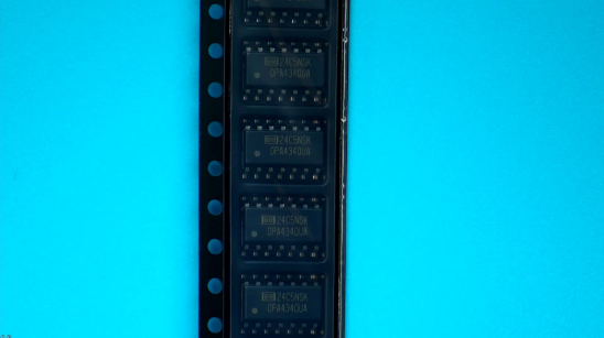
| OPA4340UA/2K5 COUNTRY OF ORIGIN |
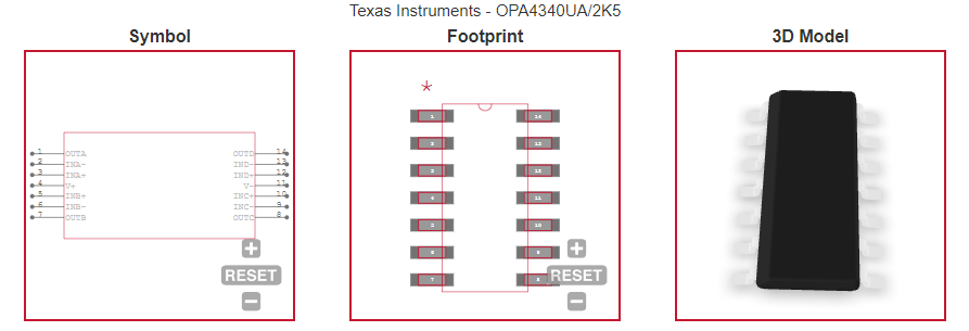
| OPA4340UA/2K5 PARAMETRIC INFO |
| OPA4340UA/2K5 PACKAGE INFO |
| OPA4340UA/2K5 MANUFACTURING INFO |
| OPA4340UA/2K5 PACKAGING INFO |
| OPA4340UA/2K5 ECAD MODELS |
| OPA4340UA/2K5 FUNCTIONAL BLOCK DIAGRAM |
| OPA4340UA/2K5 APPLICATIONS |
|
| COUNTRY OF ORIGIN |
| Malaysia |
|
| PARAMETRIC INFO |
| Manufacturer Type |
Precision Amplifier |
| Type |
Precision Amplifier |
| Rail to Rail |
Rail to Rail Input/Output |
| Minimum Single Supply Voltage (V) |
2.7 |
| Number of Channels per Chip |
4 |
| Process Technology |
CMOS |
| Minimum PSRR (dB) |
90.46(Typ) |
| Typical Single Supply Voltage (V) |
3|5 |
| Maximum Single Supply Voltage (V) |
5.5 |
| Output Type |
CMOS |
| Typical Gain Bandwidth Product (MHz) |
5.5 |
| Maximum Input Offset Voltage (mV) |
0.5@5V |
| Maximum Input Offset Current (uA) |
0.00001@5V |
| Maximum Operating Supply Voltage (V) |
5.5 |
| Maximum Input Bias Current (uA) |
0.00001@5V |
| Minimum CMRR (dB) |
70 |
| Maximum Supply Voltage Range (V) |
5.5 to 6 |
| Minimum CMRR Range (dB) |
70 to 71 |
| Typical Voltage Gain (dB) |
124 |
| Typical Slew Rate (V/us) |
6@5V |
| Typical Input Offset Current (uA) |
0.0000002@5V |
| Typical Settling Time (ns) |
1600 |
| Typical Input Noise Voltage Density (nV/rtHz) |
25@5V |
| Typical Noninverting Input Current Noise Density (pA/rtHz) |
0.003@5V |
| Typical Input Bias Current (uA) |
0.0000002@5V |
| Shut Down Support |
No |
| Minimum Operating Temperature (°C) |
-40 |
| Maximum Operating Temperature (°C) |
85 |
| Power Supply Type |
Single |
|
| |
| PACKAGE INFO |
| Supplier Package |
SOIC |
| Basic Package Type |
Lead-Frame SMT |
| Pin Count |
14 |
| Lead Shape |
Gull-wing |
| PCB |
14 |
| Tab |
N/R |
| Pin Pitch (mm) |
1.27 |
| Package Length (mm) |
8.75(Max) |
| Package Width (mm) |
4(Max) |
| Package Height (mm) |
1.5(Max) |
| Package Diameter (mm) |
N/R |
| Package Overall Length (mm) |
8.75(Max) |
| Package Overall Width (mm) |
6.2(Max) |
| Package Overall Height (mm) |
1.75(Max) |
| Seated Plane Height (mm) |
1.75(Max) |
| Mounting |
Surface Mount |
| Package Weight (g) |
N/A |
| Package Material |
Plastic |
| Package Description |
Small Outline IC |
| Package Family Name |
SO |
| Jedec |
MS-012AB |
| Package Outline |
Link to Datasheet |
|
| |
| MANUFACTURING INFO |
| MSL |
3 |
| Maximum Reflow Temperature (°C) |
260 |
| Reflow Solder Time (Sec) |
30 |
| Number of Reflow Cycle |
3 |
| Standard |
J-STD-020D |
| Reflow Temp. Source |
Link to Datasheet |
| Maximum Wave Temperature (°C) |
N/R |
| Wave Solder Time (Sec) |
N/R |
| Lead Finish(Plating) |
Au |
| Under Plating Material |
Pd over Ni |
| Terminal Base Material |
Cu Alloy |
|
| |
| PACKAGING INFO |
| Packaging Suffix |
2K5 |
| Packaging |
Tape and Reel |
| Quantity Of Packaging |
2500 |
| Reel Diameter (in) |
13 |
| Reel Width (mm) |
16.4 |
| Tape Pitch (mm) |
8 |
| Tape Width (mm) |
16 |
| Component Orientation |
Q1 |
| Packaging Document |
Link to Datasheet |
|
| |
| ECAD MODELS |
 |
|
| FUNCTIONAL BLOCK DIAGRAM |
 |
|
| APPLICATIONS |
| • Driving A/D Converters
|
| • PCMCIA Cards |
| • Data Acquisition |
| • Process Control |
| • Audio Processing
|
| • Communications |
| • Active Filters |
| • Test Equipment |
|