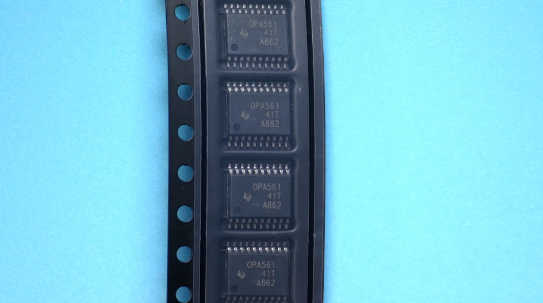
OPA561PWP Texas Instruments OPA561 High-Current, High-Speed Operational Amplifier

label:
2024/12/3 115
OPA561PWP Texas Instruments OPA561 High-Current, High-Speed Operational Amplifier


• 1.2‑A output current
• 12-VPP output voltage
• Wide power range– Single supply: 7 V to 15 V– Dual supply: ±3.5 V to ±7.5 V
• Fully protected– Thermal shutdown– Adjustable current limit
• Output disable control
• 17-MHz gain-bandwidth product
• 50-V/µs slew rate
• 1‑MHz full-power bandwidth
• Thermally enhanced HTSSOP-20 PowerPAD™ integrated circuit package
• Temperature range: 0°C to 125°C


CATALOG
OPA561PWP COUNTRY OF ORIGIN
OPA561PWP PARAMETRIC INFO
OPA561PWP PACKAGE INFO
OPA561PWP MANUFACTURING INFO
OPA561PWP PACKAGING INFO
OPA561PWP ECAD MODELS
OPA561PWP APPLICATIONS


COUNTRY OF ORIGIN
Taiwan (Province of China)
Malaysia


PARAMETRIC INFO
Manufacturer Type Wideband Amplifier
Type Wideband Amplifier
Number of Channels per Chip 1
Minimum Single Supply Voltage (V) 7
Minimum PSRR (dB) 92.04(Typ)
Typical Single Supply Voltage (V) 15
Typical Input Resistance (Ohm) 0.18T
Maximum Single Supply Voltage (V) 16
Typical Gain Bandwidth Product (MHz) 17
Minimum Dual Supply Voltage (V) ±3.5
Maximum Quiescent Current (mA) 60@15V
Maximum Input Offset Voltage (mV) 20@12V
Typical Dual Supply Voltage (V) ±5
Maximum Dual Supply Voltage (V) ±8
Maximum Input Offset Current (uA) 0.0001@15V
Maximum Input Bias Current (uA) 0.0001@15V
Maximum Operating Supply Voltage (V) ±8|16
Maximum Supply Voltage Range (V) 16 to 17
Minimum CMRR (dB) 70
Minimum CMRR Range (dB) 70 to 71
Typical Voltage Gain (dB) 100
Typical Input Offset Current (uA) 0.00001@15V
Typical Slew Rate (V/us) 50@15V
Typical Settling Time (ns) 1000
Typical Input Noise Voltage Density (nV/rtHz) 83@15V
Typical Input Bias Current (uA) 0.00001@15V
Typical Noninverting Input Current Noise Density (pA/rtHz) 0.004@15V
Shut Down Support Yes
Minimum Operating Temperature (°C) -40
Maximum Operating Temperature (°C) 125
Supplier Temperature Grade Industrial
Minimum Storage Temperature (°C) -65
Maximum Storage Temperature (°C) 150
Power Supply Type Single|Dual
Typical Output Resistance (Ohm) 0.05
Input Offset Voltage Drift (uV/°C) ±50(Typ)


PACKAGE INFO
Supplier Package HTSSOP EP
Basic Package Type Lead-Frame SMT
Pin Count 20
Lead Shape Gull-wing
PCB 20
Tab N/R
Pin Pitch (mm) 0.65
Package Length (mm) 6.6(Max)
Package Width (mm) 4.5(Max)
Package Height (mm) 1.05(Max)
Package Diameter (mm) N/R
Package Overall Length (mm) 6.6(Max)
Package Overall Width (mm) 6.6(Max)
Package Overall Height (mm) 1.2(Max)
Seated Plane Height (mm) 1.2(Max)
Mounting Surface Mount
Package Weight (g) N/A
Package Material Plastic
Package Description Heat Sinked Thin Shrink Small Outline Package, Exposed Pad
Package Family Name SO
Jedec MO-153
Package Outline Link to Datasheet


MANUFACTURING INFO
MSL 2
Maximum Reflow Temperature (°C) 260
Reflow Solder Time (Sec) 30
Number of Reflow Cycle 3
Standard J-STD-020D
Reflow Temp. Source Link to Datasheet
Maximum Wave Temperature (°C) N/R
Wave Solder Time (Sec) N/R
Wave Temp. Source Link to Datasheet
Lead Finish(Plating) Au
Under Plating Material Pd over Ni
Terminal Base Material Cu Alloy
Shelf Life Period N/A
Shelf Life Condition N/A
Number of Wave Cycles N/R


PACKAGING INFO
Packaging Tube
Quantity Of Packaging 70


ECAD MODELS


APPLICATIONS
• Power-line communications
• Valve-actuator drivers
• Power supplies
• Test equipment
• Tec drivers
Продукт RFQ