|
|
• Fully compatible with the “ISO 11898” standard
|
• High speed (up to 1 MBd)
|
• Bus lines protected against transients in an automotive environment
|
• Slope control to reduce Radio Frequency Interference (RFI)
|
• Differential receiver with wide common-mode range for high immunity againstElectroMagnetic Interference (EMI)
|
• Thermally protected
|
• Short-circuit proof to battery and ground
|
• Low-current Standby mode
|
• An unpowered node does not disturb the bus lines
|
• At least 110 nodes can be connected
|
|
| CATALOG |
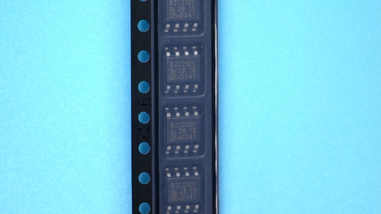
PCA82C250T/YM,118 COUNTRY OF ORIGIN
|
PCA82C250T/YM,118 PARAMETRIC INFO
|
PCA82C250T/YM,118 PACKAGE INFO
|
PCA82C250T/YM,118 MANUFACTURING INFO
|
PCA82C250T/YM,118 PACKAGING INFO
|
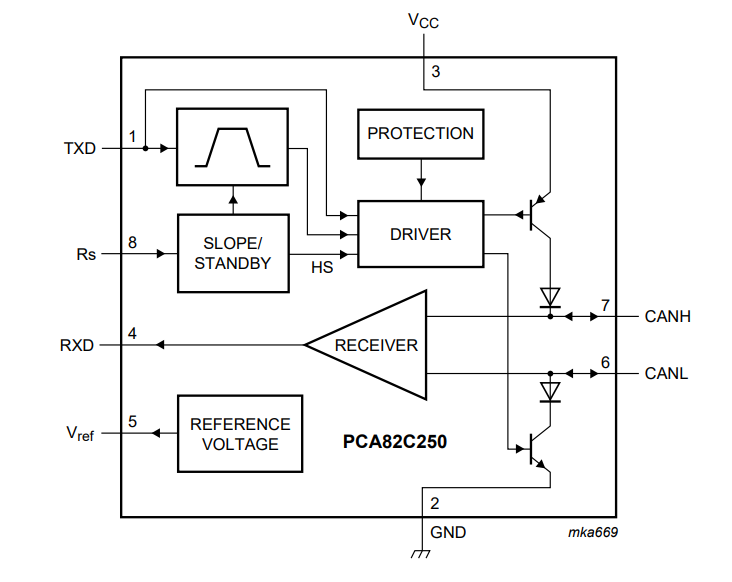
PCA82C250T/YM,118 FUNCTIONAL BLOCK DIAGRAM
|
PCA82C250T/YM,118 APPLICATIONS
|
|
COUNTRY OF ORIGIN
|
Thailand
|
Taiwan (Province of China)
|
China
|
|
PARAMETRIC INFO
|
| Category |
Transceiver |
| Maximum Data Rate |
1MBd |
| Standard Supported |
ISO 11898 |
| Number of Transceivers |
1 |
| Power Down Mode |
Standby |
| Minimum Operating Temperature (°C) |
-40 |
| Maximum Operating Temperature (°C) |
125 |
| Supplier Temperature Grade |
Automotive |
| Maximum Storage Temperature (°C) |
150 |
| Minimum Storage Temperature (°C) |
-55 |
| Typical Operating Supply Voltage (V) |
5 |
| Minimum Operating Supply Voltage (V) |
4.5 |
| Maximum Operating Supply Voltage (V) |
5.5 |
| Maximum Supply Current (mA) |
70 |
|
|
PACKAGE INFO
|
| Supplier Package |
SO |
| Pin Count |
8 |
| PCB |
8 |
| Tab |
N/R |
| Pin Pitch (mm) |
1.27 |
| Package Length (mm) |
5(Max) |
| Package Width (mm) |
4(Max) |
| Package Height (mm) |
1.45(Max) |
| Package Diameter (mm) |
N/R |
| Package Overall Length (mm) |
5(Max) |
| Package Overall Width (mm) |
6.2(Max) |
| Package Overall Height (mm) |
1.75(Max) |
| Seated Plane Height (mm) |
1.75(Max) |
| Mounting |
Surface Mount |
| Package Material |
Plastic |
| Package Family Name |
SO |
| Jedec |
MS-012AA |
| Package Outline |
Link to Datasheet |
|
|
MANUFACTURING INFO
|
| MSL |
1 |
| Maximum Reflow Temperature (°C) |
260 |
| Reflow Solder Time (Sec) |
30 |
| Number of Reflow Cycle |
3 |
| Standard |
N/A |
| Reflow Temp. Source |
Link to Datasheet |
| Maximum Wave Temperature (°C) |
N/R |
| Wave Solder Time (Sec) |
N/R |
| Lead Finish(Plating) |
Au |
| Under Plating Material |
PdNiAg |
| Terminal Base Material |
Cu Alloy |
| Number of Wave Cycles |
N/R |
|
|
PACKAGING INFO
|
|
|
|
FUNCTIONAL BLOCK DIAGRAM
|
|
|
APPLICATIONS
|
• High-speed automotive applications (up to 1 MBd).
|
|
|