|
|
• Guard Ring Die Construction for Transient Protection
|
• High Maximum Junction Temperature
|
• Very Low Leakage Current
|
• Highly Stable Oxide Passivated Junction
|
• Low Forward Voltage Drop
|
| • High Forward Surge Current Capability |
| • Lead-Free Finish; RoHS Compliant (Notes 1 & 2)
|
| • Halogen and Antimony Free. “Green” Device (Note 3) |
| • Qualified to AEC-Q101 Standards for High Reliability |
| • PPAP Capable (Note 4) |
|
| CATALOG |
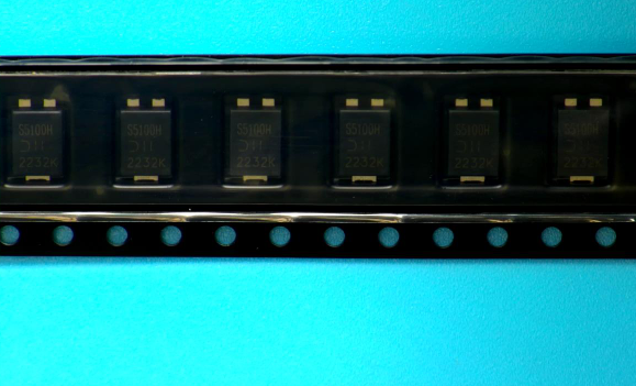
PDS5100H-13 COUNTRY OF ORIGIN
|
PDS5100H-13 PARAMETRIC INFO
|
PDS5100H-13 PACKAGE INFO
|
PDS5100H-13 MANUFACTURING INFO
|
PDS5100H-13 PACKAGING INFO
|
|
COUNTRY OF ORIGIN
|
| United Kingdom of Great Britain and Northern Ireland |
| Japan |
| United States of America |
| China |
|
PARAMETRIC INFO
|
| Type |
Schottky Diode |
| Configuration |
Single Dual Anode |
| Peak Reverse Repetitive Voltage (V) |
100 |
| Maximum DC Reverse Voltage (V) |
100 |
| Maximum Continuous Forward Current (A) |
5 |
| Maximum Power Dissipation (mW) |
2500(Typ) |
| Average Rectified Forward Current (A) |
5 |
| Maximum Junction Ambient Thermal Resistance |
85°C/W(Typ) |
| Maximum Junction Case Thermal Resistance |
5°C/W |
| Peak Forward Voltage (V) |
0.8@10A |
| Maximum RMS Reverse Voltage (V) |
71 |
| Peak Non-Repetitive Surge Current (A) |
250 |
| Peak Reverse Current (uA) |
3.5 |
| Operating Junction Temperature (°C) |
-65 to 175 |
| Minimum Storage Temperature (°C) |
-65 |
| Maximum Storage Temperature (°C) |
175 |
| Minimum Operating Temperature (°C) |
-65 |
| Maximum Operating Temperature (°C) |
175 |
| Supplier Temperature Grade |
Automotive |
|
|
PACKAGE INFO
|
| Supplier Package |
PowerDI 5 |
| Pin Count |
3 |
| PCB |
3 |
| Tab |
Tab |
| Package Length (mm) |
3.97 |
| Package Width (mm) |
5.37 |
| Package Height (mm) |
1.1(Max) |
| Package Diameter (mm) |
N/R |
| Mounting |
Surface Mount |
| Jedec |
N/A |
|
|
MANUFACTURING INFO
|
| MSL |
1 |
| Maximum Reflow Temperature (°C) |
260 |
| Reflow Solder Time (Sec) |
30 |
| Number of Reflow Cycle |
3 |
| Standard |
J-STD-020D |
| Reflow Temp. Source |
Link to Datasheet |
| Maximum Wave Temperature (°C) |
N/R |
| Wave Solder Time (Sec) |
N/R |
| Lead Finish(Plating) |
Matte Sn annealed |
| Under Plating Material |
N/A |
| Terminal Base Material |
Cu |
|
|
PACKAGING INFO
|
| Packaging Suffix |
13 |
| Packaging |
Tape and Reel |
| Quantity Of Packaging |
5000 |
| Packaging Document |
Link to Datasheet |
|
|
| |
| |