 |
|
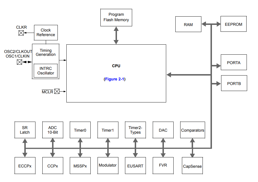
• Analog-to-Digital Converter (ADC) Module:
- 10-bit resolution, 12 channels
- Auto acquisition capability
- Conversion available during Sleep |
• Analog Comparator Module:
- Two rail-to-rail analog comparators
- Power mode control
- Software controllable hysteresis |
• Voltage Reference Module:
- Fixed Voltage Reference (FVR) with 1.024V,
2.048V and 4.096V output levels
- 5-bit rail-to-rail resistive DAC with positive
and negative reference selection |
|
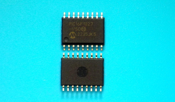
| CATALOG |
| PIC16F1827-I/SO COUNTRY OF ORIGIN |
| PIC16F1827-I/SO PARAMETRIC INFO |
| PIC16F1827-I/SO PACKAGE INFO |
| PIC16F1827-I/SO MANUFACTURING INFO |
| PIC16F1827-I/SO PACKAGING INFO |
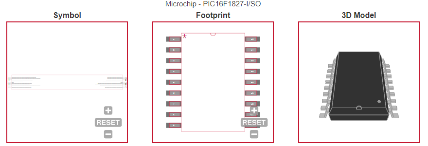
| PIC16F1827-I/SO ECAD MODELS |
| PIC16F1827-I/SO FUNCTIONAL BLOCK DIAGRAM |
|
| COUNTRY OF ORIGIN |
| Taiwan (Province of China) |
| Thailand |
| China |
|
| PARAMETRIC INFO |
| Data Bus Width (bit) |
8 |
| Family Name |
PIC16 |
| Device Core |
PIC |
| Instruction Set Architecture |
RISC |
| Maximum Clock Rate (MHz) |
32 |
| Program Memory Type |
Flash |
| Program Memory Size |
7KB |
| RAM Size |
384B |
| Maximum CPU Frequency (MHz) |
32 |
| Number of Programmable I/Os |
16 |
| Number of Timers |
5 |
| ADC Channels |
12 |
| ADC Resolution (bit) |
10 |
| Number of ADCs |
Single |
| Core Architecture |
PIC |
| PWM |
4 |
| Watchdog |
1 |
| Analog Comparators |
2 |
| Interface Type |
I2C/SPI/USART |
| Programmability |
Yes |
| SPI |
2 |
| I2C |
2 |
| I2S |
0 |
| UART |
0 |
| USART |
1 |
| CAN |
0 |
| USB |
0 |
| Ethernet |
0 |
| Maximum Power Dissipation (mW) |
800 |
| Minimum Operating Supply Voltage (V) |
1.8 |
| Typical Operating Supply Voltage (V) |
2.5|3.3|5 |
| Maximum Operating Supply Voltage (V) |
5.5 |
| Minimum Operating Temperature (°C) |
-40 |
| Maximum Operating Temperature (°C) |
85 |
| Temperature Flag |
Opr |
| Supplier Temperature Grade |
Industrial |
| Operating Supply Voltage (V) |
2.5|3.3|5 |
| Maximum Storage Temperature (°C) |
150 |
| Minimum Storage Temperature (°C) |
-65 |
|
|
| PACKAGE INFO |
| Supplier Package |
SOIC W |
| Basic Package Type |
Lead-Frame SMT |
| Pin Count |
18 |
| Lead Shape |
Gull-wing |
| PCB |
18 |
| Tab |
N/R |
| Package Length (mm) |
11.55 |
| Package Width (mm) |
7.5 |
| Package Height (mm) |
2.05(Min) |
| Package Diameter (mm) |
N/R |
| Mounting |
Surface Mount |
| Package Weight (g) |
N/A |
| Package Description |
Small Outline IC Wide Body |
| Package Family Name |
SO |
| Jedec |
MS-013AB |
| Package Outline |
Link to Datasheet |
|
|
| MANUFACTURING INFO |
| MSL |
1 |
| Maximum Reflow Temperature (°C) |
260 |
| Reflow Solder Time (Sec) |
20 to 40 |
| Number of Reflow Cycle |
3 |
| Standard |
J-STD-020C |
| Reflow Temp. Source |
Link to Datasheet |
| Maximum Wave Temperature (°C) |
N/R |
| Wave Solder Time (Sec) |
N/R |
| Wave Temp. Source |
Link to Datasheet |
| Lead Finish(Plating) |
Matte Sn annealed |
| Under Plating Material |
N/A |
| Terminal Base Material |
Cu Alloy |
|
|
| PACKAGING INFO |
| Packaging |
Tube |
| Quantity Of Packaging |
42 |
|
|
| ECAD MODELS |
 |
|
| FUNCTIONAL BLOCK DIAGRAM |
 |
| |
|