|
|
• Ultra low QG, QGD and QOSS for high system efficiency, especially at higher switching frequencies
|
• Superfast switching with soft-recovery; s-factor > 1
|
• Low spiking and ringing for low EMI designs
|
• Unique “SchottkyPlus” technology; Schottky-like performance with < 1µA leakage at 25 °C
|
• Optimised for 4.5 V gate drive
|
• Low parasitic inductance and resistance
|
• High reliability clip bonded and solder die attach Power SO8 package; no glue, no wire bonds, qualified to 175 °C
|
• Wave solderable; exposed leads for optimal visual solder inspection
|
|
| CATALOG |
PSMN2R4-30YLDX COUNTRY OF ORIGIN
|
PSMN2R4-30YLDX PARAMETRIC INFO
|
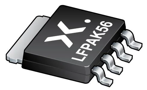
PSMN2R4-30YLDX PACKAGE INFO
|
PSMN2R4-30YLDX MANUFACTURING INFO
|
PSMN2R4-30YLDX PACKAGING INFO
|
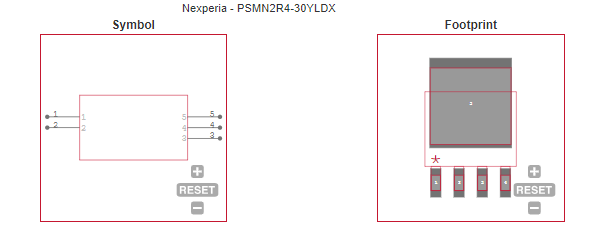
PSMN2R4-30YLDX ECAD MODELS
|
PSMN2R4-30YLDX APPLICATIONS
|
|
COUNTRY OF ORIGIN
|
China
|
Philippines
|
Malaysia
|
|
PARAMETRIC INFO
|
| Channel Type |
N |
| Channel Mode |
Enhancement |
| Configuration |
Single Triple Source |
| Maximum Drain-Source Voltage (V) |
30 |
| Maximum Absolute Continuous Drain Current (A) |
100 |
| Maximum Continuous Drain Current (A) |
100 |
| Maximum Gate-Source Voltage (V) |
20 |
| Maximum Drain-Source Resistance (mOhm) |
2.4@10V |
| Typical Gate Charge @ Vgs (nC) |
16.2@4.5V|31.3@10V |
| Operating Junction Temperature (°C) |
-55 to 175 |
| Typical Gate Charge @ 10V (nC) |
31.3 |
| Maximum Power Dissipation (mW) |
106000 |
| Process Technology |
NextPowerS3 |
| Category |
Power MOSFET |
| Typical Input Capacitance @ Vds (pF) |
2256@15V |
| Typical Turn-On Delay Time (ns) |
16.3 |
| Typical Turn-Off Delay Time (ns) |
17.4 |
| Typical Fall Time (ns) |
13.9 |
| Typical Rise Time (ns) |
27.5 |
| Maximum Gate-Source Leakage Current (nA) |
100 |
| Maximum Gate Threshold Voltage (V) |
2.2 |
| Maximum IDSS (uA) |
1 |
| Number of Elements per Chip |
1 |
| Minimum Storage Temperature (°C) |
-55 |
| Maximum Storage Temperature (°C) |
175 |
| Minimum Operating Temperature (°C) |
-55 |
| Maximum Operating Temperature (°C) |
175 |
|
|
PACKAGE INFO
|
| Supplier Package |
LFPAK |
| Pin Count |
5 |
| PCB |
4 |
| Tab |
Tab |
| Package Length (mm) |
5(Max) |
| Package Width (mm) |
4.1(Max) |
| Package Height (mm) |
1.1(Max) |
| Package Diameter (mm) |
N/R |
| Mounting |
Surface Mount |
| Jedec |
MO-235 |
| Package Outline |
Link to Datasheet |
|
|
MANUFACTURING INFO
|
| MSL |
1 |
| Maximum Reflow Temperature (°C) |
260 |
| Reflow Solder Time (Sec) |
30 |
| Number of Reflow Cycle |
3 |
| Reflow Temp. Source |
Link to Datasheet |
| Lead Finish(Plating) |
Sn |
| Under Plating Material |
N/A |
| Terminal Base Material |
Cu Alloy |
|
|
PACKAGING INFO
|
| Packaging Suffix |
X |
| Packaging |
Tape and Reel |
|
| |
| ECAD MODELS |
 |
|
| APPLICATIONS |
| • On-board DC-to-DC solutions for server and telecommunications |
| • Secondary-side synchronous rectification in telecommunication applications |
| • Voltage regulator modules (VRM) |
| • Point-of-Load (POL) modules |
| • Power delivery for V-core, ASIC, DDR, GPU, VGA and system components |
| • Brushed and brushless motor control |
| |