|
|
• Output voltage: 1.2 V to 5.2 V, selectable in 0.05 V step
|
• Input voltage: 1.7 V to 6.5 V
|
• Output voltage accuracy: 1.0% (1.2 V to 1.45 V output product: 15 mV)
|
•Dropout voltage: 150 mV typ. (3.0 V output product, IOUT = 100 mA)
|
•Current consumption: During operation: 1.0 A typ., 1.5 A max.
|
•Output current: Possible to output 250 mA (3.0 V output product, VIN VOUT(S) 1.0 V)*1
|
• Input and output capacitors: A ceramic capacitor of 0.1 F or more can be used.
|
• Built-in overcurrent protection circuit: Limits overcurrent of output transistor.
|
•Operation temperature range: Ta = 40°C to 85°C
|
•Lead-free, Sn 100%, halogen-free*2
|
|
| CATALOG |
S-1206B33-U3T1G COUNTRY OF ORIGIN
|
S-1206B33-U3T1G PARAMETRIC INFO
|
S-1206B33-U3T1G PACKAGE INFO
|
S-1206B33-U3T1G MANUFACTURING INFO
|
S-1206B33-U3T1G PACKAGING INFO
|
S-1206B33-U3T1G APPLICATIONS
|
|
COUNTRY OF ORIGIN
|
Japan
|
|
PARAMETRIC INFO
|
| Type |
LDO |
| Number of Outputs |
1 |
| Maximum Output Current (A) |
0.25(Min) |
| Minimum Operating Temperature (°C) |
-40 |
| Maximum Operating Temperature (°C) |
85 |
| Output Voltage Range (V) |
1.8 to 10 |
| Output Type |
Fixed |
| Polarity |
Positive |
| Special Features |
Current Limit |
| Load Regulation |
40mV |
| Line Regulation |
0.2%/V |
| Maximum Dropout Voltage @ Current (V) |
0.23@100mA |
| Maximum Power Dissipation (mW) |
1000 |
| Minimum Input Voltage (V) |
1.7 |
| Maximum Input Voltage (V) |
6.5 |
| Output Voltage (V) |
3.3 |
| Typical Dropout Voltage @ Current (V) |
0.15@100mA |
| Accuracy (%) |
±1 |
|
|
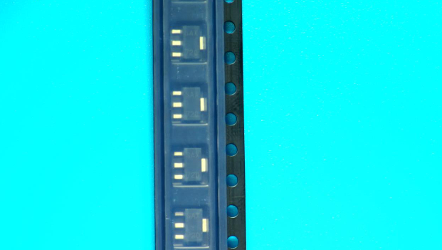
PACKAGE INFO
|
| Supplier Package |
SOT-89 |
| Basic Package Type |
Lead-Frame SMT |
| Pin Count |
4 |
| Lead Shape |
Flat |
| PCB |
3 |
| Tab |
Tab |
| Pin Pitch (mm) |
1.5 |
| Package Length (mm) |
4.5 |
| Package Width (mm) |
2.5 |
| Package Height (mm) |
1.5 |
| Package Diameter (mm) |
N/R |
| Seated Plane Height (mm) |
1.5 |
| Mounting |
Surface Mount |
| Package Material |
Plastic |
| Package Description |
Small Outline Transistor |
| Package Family Name |
SOT |
| Jedec |
TO-243AA |
| Package Outline |
Link to Datasheet |
|
|
MANUFACTURING INFO
|
| MSL |
N/A |
| Maximum Reflow Temperature (°C) |
260 |
| Reflow Solder Time (Sec) |
10 |
| Reflow Temp. Source |
Link to Datasheet |
| Maximum Wave Temperature (°C) |
N/R |
| Wave Solder Time (Sec) |
N/R |
| Wave Temp. Source |
Link to Datasheet |
| Lead Finish(Plating) |
SnBi|SnAg |
| Under Plating Material |
N/A |
| Terminal Base Material |
N/A |
|
|
PACKAGING INFO
|
| Packaging Suffix |
T1 |
| Packaging |
Tape and Reel |
|
|
APPLICATIONS
|
• Constant-voltage power supply for battery-powered device
|
| • Constant-voltage power supply for cellular phone |
• Constant-voltage power supply for portable equipment
|
| |