 |
|
| • Inputs are TTL-voltage compatible |
| • Latch-up performance exceeds 250 mA per JESD
17 |
• ESD protection exceeds JESD 22
– 2000-V Human-Body Model (A114-A)
– 200-V Machine Model (A115-A)
– 1000-V Charged-Device Model (C101) |
| • On products compliant to MIL-PRF-38535,
all parameters are tested unless otherwise noted.
On all other products, production processing does
not necessarily include testing of all parameters. |
|
| CATALOG |
| SN74AHCT14PWR COUNTRY OF ORIGIN |
| SN74AHCT14PWR PARAMETRIC INFO |
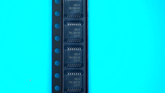
| SN74AHCT14PWR PACKAGE INFO |
| SN74AHCT14PWR MANUFACTURING INFO |
| SN74AHCT14PWR PACKAGING INFO |
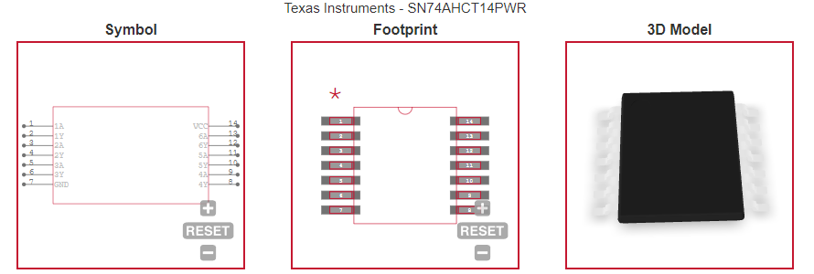
| SN74AHCT14PWR ECAD MODELS |
| SN74AHCT14PWR FUNCTIONAL BLOCK DIAGRAM |
| SN74AHCT14PWR APPLICATIONS
|
|
| COUNTRY OF ORIGIN |
| Japan |
| Malaysia |
| Philippines |
|
| PARAMETRIC INFO |
| Logic Family |
AHCT |
| Process Technology |
CMOS |
| Logic Function |
Inverter Schmitt Trigger |
| Input Type |
Schmitt Trigger |
| Output Type |
Push-Pull |
| Number of Elements per Chip |
6 |
| Minimum Operating Supply Voltage (V) |
4.5 |
| Maximum Operating Supply Voltage (V) |
5.5 |
| Typical Operating Supply Voltage (V) |
5 |
| Minimum Operating Temperature (°C) |
-40 |
| Maximum Operating Temperature (°C) |
85 |
| Supplier Temperature Grade |
Commercial |
| Maximum Propagation Delay Time @ Maximum CL (ns) |
8@5V |
| Absolute Propagation Delay Time (ns) |
9 |
| Propagation Delay Test Condition (pF) |
50 |
| Maximum High Level Output Current (mA) |
-8 |
| Maximum Low Level Output Current (mA) |
8 |
| Maximum Quiescent Current (uA) |
2 |
|
| PACKAGE INFO |
| Supplier Package |
TSSOP |
| Basic Package Type |
Lead-Frame SMT |
| Pin Count |
14 |
| Lead Shape |
Gull-wing |
| PCB |
14 |
| Tab |
N/R |
| Pin Pitch (mm) |
0.65 |
| Package Length (mm) |
5.1(Max) |
| Package Width (mm) |
4.5(Max) |
| Package Height (mm) |
1.05(Max) |
| Package Diameter (mm) |
N/R |
| Package Overall Length (mm) |
5.1(Max) |
| Package Overall Width (mm) |
6.6(Max) |
| Package Overall Height (mm) |
1.2(Max) |
| Seated Plane Height (mm) |
1.2(Max) |
| Mounting |
Surface Mount |
| Package Weight (g) |
N/A |
| Package Material |
Plastic |
| Package Description |
Thin Shrink Small Outline Package |
| Package Family Name |
SOP |
| Jedec |
MO-153AB-1 |
| Package Outline |
Link to Datasheet |
|
| MANUFACTURING INFO |
| MSL |
1 |
| Maximum Reflow Temperature (°C) |
260 |
| Reflow Solder Time (Sec) |
30 |
| Number of Reflow Cycle |
3 |
| Standard |
J-STD-020D |
| Reflow Temp. Source |
Link to Datasheet |
| Maximum Wave Temperature (°C) |
N/R |
| Wave Solder Time (Sec) |
N/R |
| Lead Finish(Plating) |
Au |
| Under Plating Material |
Pd over Ni |
| Terminal Base Material |
Cu Alloy |
| Number of Wave Cycles |
N/R |
|
| PACKAGING INFO |
| Packaging Suffix |
R |
| Packaging |
Tape and Reel |
| Quantity Of Packaging |
2000 |
| Reel Diameter (in) |
13 |
| Reel Width (mm) |
12.4 |
| Tape Pitch (mm) |
8 |
| Tape Width (mm) |
12 |
| Component Orientation |
Q1 |
| Packaging Document |
Link to Datasheet |
|
| ECAD MODELS |
 |
|
| FUNCTIONAL BLOCK DIAGRAM |
 |
|
| APPLICATIONS |
| • Servers |
| • Network switches |
| • Telecom infrastructures |
| • Tests and measurements |
|