|
|
• Operating range of 4.5 V to 5.5 V
|
• Low power consumption, 10-µA maximum ICC
|
• ±8-mA output drive at 5 V
|
• Inputs are TTL-voltage compatible
|
• Latch-up performance exceeds 250 mA per JESD 17
|
|
| CATALOG |
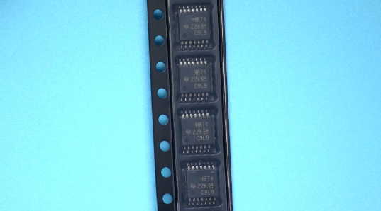
SN74AHCT74PWR COUNTRY OF ORIGIN
|
SN74AHCT74PWR PARAMETRIC INFO
|
SN74AHCT74PWR PACKAGE INFO
|
SN74AHCT74PWR MANUFACTURING INFO
|
SN74AHCT74PWR PACKAGING INFO
|
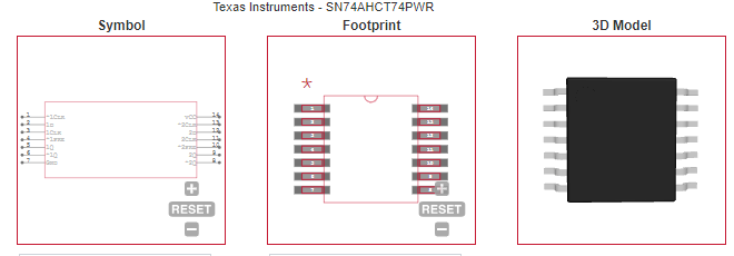
SN74AHCT74PWR ECAD MODELS
|
SN74AHCT74PWR APPLICATIONS
|
|
COUNTRY OF ORIGIN
|
China
|
Taiwan (Province of China)
|
Malaysia
|
Philippines
|
|
PARAMETRIC INFO
|
| Logic Family |
AHCT |
| Process Technology |
CMOS |
| Logic Function |
D-Type |
| Bus Hold |
No |
| Number of Elements per Chip |
2 |
| Maximum Frequency (50pF, 25°C) @ Vcc (MHz) |
140(Typ)@5V |
| Maximum Frequency (15pF, 25°C) @ Vcc (MHz) |
160(Typ)@5V |
| Maximum Propagation Delay (50pF, 25°C) @ Vcc (ns) |
8.8@5V |
| Maximum Propagation Delay (15pF, 25°C) @ Vcc (ns) |
7.8@5V |
| Number of Channels per Chip |
2 |
| Number of Element Inputs |
1 |
| Number of Element Outputs |
1 |
| Set/Reset |
Set/Reset |
| Input Signal Type |
Single-Ended |
| Output Signal Type |
Differential |
| Output Type |
Push-Pull |
| Triggering Type |
Positive-Edge |
| Polarity |
Inverting/Non-Inverting |
| Minimum Operating Supply Voltage (V) |
4.5 |
| Typical Operating Supply Voltage (V) |
5 |
| Maximum Operating Supply Voltage (V) |
5.5 |
| Minimum Operating Temperature (°C) |
-40 |
| Maximum Operating Temperature (°C) |
125 |
| Supplier Temperature Grade |
Commercial |
| Minimum Storage Temperature (°C) |
-65 |
| Maximum Storage Temperature (°C) |
150 |
| Maximum Propagation Delay Time @ Maximum CL (ns) |
8.8@5V |
| Absolute Propagation Delay Time (ns) |
13 |
| Propagation Delay Test Condition (pF) |
50 |
| Maximum High Level Output Current (mA) |
-8 |
| Maximum Low Level Output Current (mA) |
8 |
| Maximum Quiescent Current (mA) |
0.002 |
|
|
PACKAGE INFO
|
| Supplier Package |
TSSOP |
| Basic Package Type |
Lead-Frame SMT |
| Pin Count |
14 |
| Lead Shape |
Gull-wing |
| PCB |
14 |
| Tab |
N/R |
| Pin Pitch (mm) |
0.65 |
| Package Length (mm) |
5.1(Max) |
| Package Width (mm) |
4.5(Max) |
| Package Height (mm) |
1.05(Max) |
| Package Diameter (mm) |
N/R |
| Package Overall Length (mm) |
5.1(Max) |
| Package Overall Width (mm) |
6.6(Max) |
| Package Overall Height (mm) |
1.2(Max) |
| Seated Plane Height (mm) |
1.2(Max) |
| Mounting |
Surface Mount |
| Package Weight (g) |
N/A |
| Package Material |
Plastic |
| Package Description |
Thin Shrink Small Outline Package |
| Package Family Name |
SO |
| Jedec |
MO-153AB-1 |
| Package Outline |
Link to Datasheet |
|
|
MANUFACTURING INFO
|
| MSL |
1 |
| Maximum Reflow Temperature (°C) |
260 |
| Reflow Solder Time (Sec) |
30 |
| Number of Reflow Cycle |
3 |
| Standard |
J-STD-020D |
| Reflow Temp. Source |
Link to Datasheet |
| Maximum Wave Temperature (°C) |
N/R |
| Wave Solder Time (Sec) |
N/R |
| Lead Finish(Plating) |
Matte Sn|Au |
| Under Plating Material |
N/A|Pd over Ni |
| Terminal Base Material |
Cu Alloy |
|
|
PACKAGING INFO
|
| Packaging Suffix |
R |
| Packaging |
Tape and Reel |
| Quantity Of Packaging |
2000 |
| Reel Diameter (in) |
13 |
| Reel Width (mm) |
12.4 |
| Tape Pitch (mm) |
8 |
| Tape Width (mm) |
12 |
| Component Orientation |
Q1 |
| Packaging Document |
Link to Datasheet |
|
|
| ECAD MODELS |
 |
|
| APPLICATIONS |
| • Convert a momentary switch to a toggle switch |
| • Hold a signal during controller reset |
| • Input slow edge-rate signals |
| • Operate in noisy environments |
| • Divide a clock signal by two |
| |