 |
|
| • 8-bit serial-in, parallel-out shift |
| • Wide operating voltage range of 2 V to 6 V |
| • High-current 3-state outputs can drive up to 15
LSTTL loads |
| • Low power consumption: 80-μA (maximum) ICC |
| • tpd = 13 ns (typical)
|
| • ±6-mA output drive at 5 V |
| • Low input current: 1 μA (maximum)
|
| • Shift register has direct clear |
| • On products compliant to MIL-PRF-38535,
all parameters are tested unless otherwise noted.
On all other products, production processing does
not necessarily include testing of all parameters.
|
|
| CATALOG |
| SN74HC595DR COUNTRY OF ORIGIN |
| SN74HC595DR PARAMETRIC INFO |
| SN74HC595DR PACKAGE INFO |
| SN74HC595DR MANUFACTURING INFO |
| SN74HC595DR PACKAGING INFO |
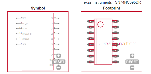
| SN74HC595DR ECAD MODELS |
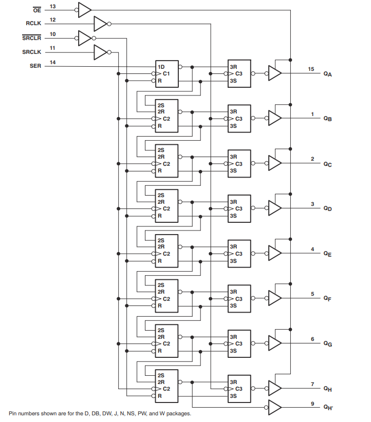
| SN74HC595DR FUNCTIONAL BLOCK DIAGRAM
|
| SN74HC595DR APPLICATIONS |
|
| COUNTRY OF ORIGIN |
| Taiwan (Province of China) |
| Malaysia |
| Mexico |
| China |
| Philippines |
|
| PARAMETRIC INFO |
| Logic Function |
Shift Register |
| Logic Family |
HC |
| Process Technology |
CMOS |
| Number of Count Input Enables |
0 |
| Number of Element Inputs |
1 |
| Number of Element Outputs |
9 |
| Number of Elements per Chip |
1 |
| Number of Selection Inputs per Element |
0 |
| Number of Stages |
8 |
| Operation Mode |
Serial to Serial/Parallel |
| Output Type |
3-State |
| Reset Type |
Asynchronous |
| Direction Type |
Uni-Directional |
| Terminal Count Output |
No |
| Triggering Type |
Positive-Edge |
| Minimum Operating Supply Voltage (V) |
2 |
| Maximum Operating Supply Voltage (V) |
6 |
| Typical Operating Supply Voltage (V) |
5 |
| Minimum Operating Temperature (°C) |
-40 |
| Maximum Operating Temperature (°C) |
85 |
| Maximum Propagation Delay Time @ Maximum CL (ns) |
200@2V|40@4.5V|34@6V |
| Absolute Propagation Delay Time (ns) |
250 |
| Propagation Delay Test Condition (pF) |
150 |
| Maximum Quiescent Current (mA) |
0.008 |
| Minimum Storage Temperature (°C) |
-65 |
| Maximum Storage Temperature (°C) |
150 |
| Parallel Enable Input |
No |
|
|
PACKAGE INFO
|
| Supplier Package |
SOIC |
| Basic Package Type |
Lead-Frame SMT |
| Pin Count |
16 |
| Lead Shape |
Gull-wing |
| PCB |
16 |
| Tab |
N/R |
| Pin Pitch (mm) |
1.27 |
| Package Length (mm) |
10(Max) |
| Package Width (mm) |
4(Max) |
| Package Height (mm) |
1.5(Max) |
| Package Diameter (mm) |
N/R |
| Package Overall Length (mm) |
10(Max) |
| Package Overall Width (mm) |
6.2(Max) |
| Package Overall Height (mm) |
1.75(Max) |
| Seated Plane Height (mm) |
1.75(Max) |
| Mounting |
Surface Mount |
| Package Weight (g) |
N/A |
| Package Material |
Plastic |
| Package Description |
Small Outline IC |
| Package Family Name |
SO |
| Jedec |
MS-012AC |
| Package Outline |
Link to Datasheet |
|
| |
| MANUFACTURING INFO |
| MSL |
1 |
| Maximum Reflow Temperature (°C) |
260 |
| Reflow Solder Time (Sec) |
30 |
| Number of Reflow Cycle |
3 |
| Standard |
J-STD-020D |
| Reflow Temp. Source |
Link to Datasheet |
| Maximum Wave Temperature (°C) |
N/R |
| Wave Solder Time (Sec) |
N/R |
| Lead Finish(Plating) |
Matte Sn|Au |
| Under Plating Material |
N/A|Pd over Ni |
| Terminal Base Material |
N/A|Cu Alloy |
| Number of Wave Cycles |
N/R |
|
| |
| PACKAGING INFO |
| Packaging Suffix |
R |
| Packaging |
Tape and Reel |
| Quantity Of Packaging |
2500 |
| Reel Diameter (in) |
13 |
| Reel Width (mm) |
16.4|16.8 |
| Tape Pitch (mm) |
8 |
| Tape Width (mm) |
16 |
| Component Orientation |
Q1 |
| Packaging Document |
Link to Datasheet |
|
| |
| ECAD MODELS |
 |
|
| FUNCTIONAL BLOCK DIAGRAM |
 |
|
| APPLICATIONS |
| • Network switches |
| • Power infrastructure |
| • LED displays |
| • Servers |
| |
| |