|
|
• VCC operation of 2 V to 5.5 V
|
• Maximum tpd of 7.1 ns at 5 V
|
• Typical VOLP (output ground bounce)
|
• Typical VOLP (output ground bounce)
< 0.8 V at VCC = 3.3 V, TA = 25°C
|
• Typical VOHV (output VOH undershoot)
> 2.3 V at VCC = 3.3 V, TA = 25°C
|
| • Support mixed-mode voltage operation on all ports |
| • 8-bit serial-in, parallel-out shift |
| • Ioff supports live insertion, partial power-down
mode, and back-drive protection |
| • Shift register has direct clear |
| • Latch-up performance exceeds 250 mA per JESD
17 |
|
| CATALOG |
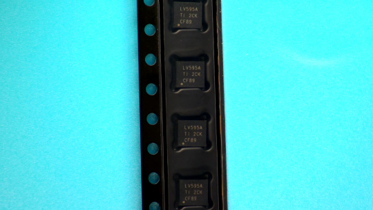
SN74LV595ARGYR COUNTRY OF ORIGIN
|
SN74LV595ARGYR PARAMETRIC INFO
|
SN74LV595ARGYR PACKAGE INFO
|
SN74LV595ARGYR MANUFACTURING INFO
|
SN74LV595ARGYR PACKAGING INFO
|
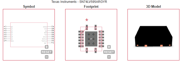
SN74LV595ARGYR ECAD MODELS
|
SN74LV595ARGYR APPLICATIONS
|
|
COUNTRY OF ORIGIN
|
United States of America
|
China
|
Malaysia
|
|
PARAMETRIC INFO
|
| Logic Function |
Shift Register |
| Logic Family |
LV |
| Process Technology |
CMOS |
| Number of Count Input Enables |
0 |
| Number of Element Inputs |
1 |
| Number of Element Outputs |
9 |
| Number of Elements per Chip |
1 |
| Number of Selection Inputs per Element |
0 |
| Number of Stages |
8 |
| Operation Mode |
Serial to Serial/Parallel |
| Output Type |
3-State |
| Direction Type |
Uni-Directional |
| Terminal Count Output |
No |
| Tolerant I/Os (V) |
5 Inputs |
| Triggering Type |
Positive-Edge |
| Minimum Operating Supply Voltage (V) |
2 |
| Maximum Operating Supply Voltage (V) |
5.5 |
| Typical Operating Supply Voltage (V) |
2.5|3.3|5 |
| Minimum Operating Temperature (°C) |
-40 |
| Maximum Operating Temperature (°C) |
125 |
| Supplier Temperature Grade |
Commercial |
| Maximum Propagation Delay Time @ Maximum CL (ns) |
22.5@2.5V|16.5@3.3V|10.2@5V |
| Absolute Propagation Delay Time (ns) |
27.5 |
| Propagation Delay Test Condition (pF) |
50 |
| Maximum Quiescent Current (mA) |
0.02 |
| Minimum Storage Temperature (°C) |
-65 |
| Maximum Storage Temperature (°C) |
150 |
| Parallel Enable Input |
No |
|
|
PACKAGE INFO
|
| Supplier Package |
VQFN EP |
| Basic Package Type |
Non-Lead-Frame SMT |
| Pin Count |
16 |
| Lead Shape |
No Lead |
| PCB |
16 |
| Tab |
N/R |
| Pin Pitch (mm) |
0.5 |
| Package Length (mm) |
4.15(Max) |
| Package Width (mm) |
3.65(Max) |
| Package Height (mm) |
0.95(Max) |
| Package Diameter (mm) |
N/R |
| Seated Plane Height (mm) |
1(Max) |
| Mounting |
Surface Mount |
| Package Weight (g) |
N/A |
| Package Material |
Plastic |
| Package Description |
Very Thin Quad Flat No Lead Package, Exposed Pad |
| Package Family Name |
QFN |
| Jedec |
MO-241-BA |
|
|
MANUFACTURING INFO
|
| MSL |
2 |
| Maximum Reflow Temperature (°C) |
260 |
| Reflow Solder Time (Sec) |
30 |
| Number of Reflow Cycle |
3 |
| Standard |
J-STD-020D |
| Reflow Temp. Source |
Link to Datasheet |
| Maximum Wave Temperature (°C) |
N/R |
| Wave Solder Time (Sec) |
N/R |
| Wave Temp. Source |
Link to Datasheet |
| Lead Finish(Plating) |
Au |
| Under Plating Material |
Pd over Ni |
| Terminal Base Material |
Cu Alloy |
| Shelf Life Period |
N/A |
| Shelf Life Condition |
N/A |
| Number of Wave Cycles |
N/R |
|
|
PACKAGING INFO
|
| Packaging Suffix |
R |
| Packaging |
Tape and Reel |
| Quantity Of Packaging |
3000 |
| Reel Diameter (in) |
13 |
| Reel Width (mm) |
12.4 |
| Tape Pitch (mm) |
8 |
| Tape Width (mm) |
12 |
| Component Orientation |
Q1 |
| Packaging Document |
Link to Datasheet |
|
|
ECAD MODELS
|
|
|
APPLICATIONS
|
• Output expansion
|
| • LED matrix control |
• 7-segment display control
|
|
| |