|
|
• Latch-up performance exceeds 100 mA per JESD 78, Class II
|
• ESD protection exceeds JESD 22– 2000-V human-body model (A114-A)– 200-V machine model (A115-A)– 1000-V charged-device model (C101)
|
• Operate from 1.65 V to 3.6 V VCC
|
• Specified from –40°C to +85°C,–40°C to 125°C, and –55°C to 125°C
|
• Inputs accept voltages to 5.5 V
|
• Max tpd of 6.4 ns at 3.3 V
|
• Typical VOLP (output ground bounce)<0.8 V at VCC = 3.3 V, TA = 25°C
|
• Typical VOHV (output VOH undershoot)>2 V at VCC = 3.3 V, TA = 25°C
|
• On products compliant to MIL-PRF-38535,all parameters are tested unless otherwise noted.On all other products, production processing does not necessarily include testing of all parameters.
|
|
| CATALOG |
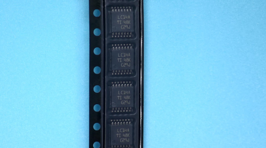
SN74LVC14APWR COUNTRY OF ORIGIN
|
SN74LVC14APWR PARAMETRIC INFO
|
SN74LVC14APWR PACKAGE INFO
|
SN74LVC14APWR MANUFACTURING INFO
|
SN74LVC14APWR PACKAGING INFO
|
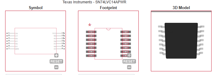
SN74LVC14APWR ECAD MODELS
|
SN74LVC14APWR APPLICATIONS
|
|
COUNTRY OF ORIGIN
|
China
|
Taiwan (Province of China)
|
Malaysia
|
|
PARAMETRIC INFO
|
| Type |
LDO |
| Number of Outputs |
1 |
| Maximum Output Current (A) |
0.8 |
| Minimum Operating Temperature (°C) |
-40 |
| Maximum Operating Temperature (°C) |
125 |
| Regulation Condition Change In Line |
13V |
| Output Type |
Adjustable |
| Output Voltage Range (V) |
<1.8|1.8 to 10 |
| Junction to Ambient |
38.1°C/W |
| Junction to Case |
27.9°C/W |
| Polarity |
Positive |
| Special Features |
Current Limit|Thermal Protection |
| Line Regulation |
0.01%/V(Typ) |
| Maximum Dropout Voltage @ Current (V) |
0.002@100uA|0.2@200mA|0.6@800mA |
| Minimum Input Voltage (V) |
2.5 |
| Maximum Input Voltage (V) |
16 |
| Output Voltage (V) |
1 to 5.5 |
| Typical Quiescent Current (mA) |
5.5 |
| Typical Dropout Voltage @ Current (V) |
0.001@100uA|0.15@200mA|0.475@800mA |
| Accuracy (%) |
±1 |
| Minimum Storage Temperature (°C) |
-65 |
| Maximum Storage Temperature (°C) |
150 |
| Typical Ground Current @ Full Load (mA) |
5.5 |
| Typical PSRR (dB) |
60 |
| Typical Output Noise Voltage (uVrms) |
18 |
| Output Capacitor Type |
Ceramic |
|
|
PACKAGE INFO
|
| Supplier Package |
WSON EP |
| Basic Package Type |
Non-Lead-Frame SMT |
| Pin Count |
8 |
| Lead Shape |
No Lead |
| PCB |
8 |
| Tab |
N/R |
| Pin Pitch (mm) |
0.8 |
| Package Length (mm) |
4.1(Max) |
| Package Width (mm) |
4.1(Max) |
| Package Height (mm) |
0.75(Max) |
| Package Diameter (mm) |
N/R |
| Package Overall Length (mm) |
4.1(Max) |
| Package Overall Width (mm) |
4.1(Max) |
| Package Overall Height (mm) |
0.8(Max) |
| Seated Plane Height (mm) |
0.8(Max) |
| Mounting |
Surface Mount |
| Package Weight (g) |
N/A |
| Package Material |
Plastic |
| Package Description |
Very Very Thin Small Outline No Lead Package, Exposed Pad |
| Package Family Name |
SON |
| Jedec |
N/A |
| Package Outline |
Link to Datasheet |
|
|
MANUFACTURING INFO
|
| MSL |
1 |
| Maximum Reflow Temperature (°C) |
260 |
| Reflow Solder Time (Sec) |
30 |
| Number of Reflow Cycle |
3 |
| Standard |
J-STD-020D |
| Reflow Temp. Source |
Link to Datasheet |
| Maximum Wave Temperature (°C) |
N/R |
| Wave Solder Time (Sec) |
N/R |
| Lead Finish(Plating) |
Matte Sn|Au |
| Under Plating Material |
N/A|Pd over Ni |
| Terminal Base Material |
Cu Alloy|N/A |
| Number of Wave Cycles |
N/R |
|
|
PACKAGING INFO
|
| Packaging |
Tape and Reel |
| Quantity Of Packaging |
1000 |
| Reel Diameter (in) |
7.09 |
| Reel Width (mm) |
12.4 |
| Tape Pitch (mm) |
8 |
| Tape Width (mm) |
12 |
| Component Orientation |
Q1 |
| Packaging Document |
Link to Datasheet |
|
|
ECAD MODELS
|
|
|
| APPLICATIONS |
| • Barcode scanner |
| • Cable solutions |
| |