|
|
• Qualified for Automotive Applications
|
• Supports 5-V VCC operation
|
• Inputs accept voltages to 5.5 V
|
• Max tpd of 8 ns at 3.3 V
|
• Low power consumption, 20-μA Max ICC
|
• ±24-mA Output drive at 3.3 V
|
• Ioff Supports live insertion, partial-power-down
mode, and back-drive protection
|
• ESD protection exceeds JEDEC JS-001
– 2000-V Human-body model
– 1000-V Charged-device mode
|
|
| CATALOG |
SN74LVC1G17QDBVRQ1 COUNTRY OF ORIGIN
|
SN74LVC1G17QDBVRQ1 PARAMETRIC INFO
|
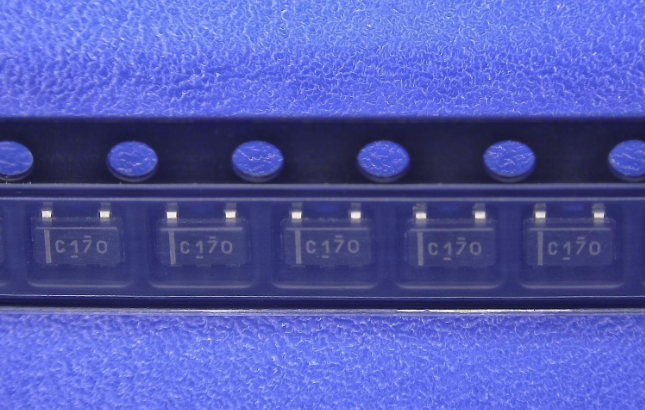
SN74LVC1G17QDBVRQ1 PACKAGE INFO
|
SN74LVC1G17QDBVRQ1 MANUFACTURING INFO
|
SN74LVC1G17QDBVRQ1 PACKAGING INFO
|
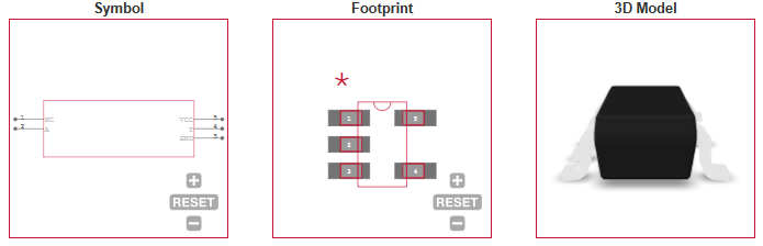
SN74LVC1G17QDBVRQ1 ECAD MODELS
|
SN74LVC1G17QDBVRQ1 APPLICATIONS
|
|
COUNTRY OF ORIGIN
|
China
|
Malaysia
|
Thailand
|
|
PARAMETRIC INFO
|
| Process Technology |
CMOS |
| Logic Family |
LVC |
| Logic Function |
Schmitt Trigger Buffer |
| Input Signal Type |
Single-Ended |
| Output Type |
Push-Pull |
| Polarity |
Non-Inverting |
| Tolerant I/Os (V) |
5 |
| Bus Hold |
No |
| Number of Elements per Chip |
1 |
| Number of Channels per Chip |
1 |
| Number of Output Enables per Chip |
0 |
| Number of Input Enables per Chip |
0 |
| Number of Inputs per Chip |
1 |
| Number of Outputs per Chip |
1 |
| Minimum Operating Supply Voltage (V) |
1.65 |
| Maximum Operating Supply Voltage (V) |
5.5 |
| Typical Operating Supply Voltage (V) |
1.8|2.5|3.3|5 |
| Minimum Operating Temperature (°C) |
-40 |
| Maximum Operating Temperature (°C) |
125 |
| Supplier Temperature Grade |
Automotive |
| Maximum Propagation Delay Time @ Maximum CL (ns) |
8@3.3V|7@5V |
| Absolute Propagation Delay Time (ns) |
14 |
| Propagation Delay Test Condition (pF) |
50 |
| Maximum High Level Output Current (mA) |
-32 |
| Maximum Low Level Output Current (mA) |
32 |
| Maximum Quiescent Current (uA) |
20 |
|
|
PACKAGE INFO
|
| Supplier Package |
SOT-23 |
| Basic Package Type |
Lead-Frame SMT |
| Pin Count |
5 |
| Lead Shape |
Gull-wing |
| PCB |
5 |
| Tab |
N/R |
| Pin Pitch (mm) |
0.95 |
| Package Length (mm) |
3.05(Max) |
| Package Width (mm) |
1.75(Max) |
| Package Height (mm) |
1.1 |
| Package Diameter (mm) |
N/R |
| Package Overall Length (mm) |
3.05(Max) |
| Package Overall Width (mm) |
3(Max) |
| Package Overall Height (mm) |
1.45(Max) |
| Seated Plane Height (mm) |
1.45(Max) |
| Mounting |
Surface Mount |
| Package Weight (g) |
N/A |
| Package Material |
Plastic |
| Package Description |
Small Outline Transistor |
| Package Family Name |
SOT |
| Jedec |
MO-178AA |
| Package Outline |
Link to Datasheet |
|
|
MANUFACTURING INFO
|
| MSL |
1 |
| Maximum Reflow Temperature (°C) |
260 |
| Reflow Solder Time (Sec) |
30 |
| Number of Reflow Cycle |
3 |
| Standard |
J-STD-020D |
| Reflow Temp. Source |
Link to Datasheet |
| Maximum Wave Temperature (°C) |
N/R |
| Wave Solder Time (Sec) |
N/R |
| Lead Finish(Plating) |
Au |
| Under Plating Material |
Pd over Ni |
| Terminal Base Material |
Cu Alloy |
|
|
PACKAGING INFO
|
| Packaging Suffix |
R |
| Packaging |
Tape and Reel |
| Quantity Of Packaging |
3000 |
| Reel Diameter (in) |
7 |
| Tape Pitch (mm) |
4 |
| Tape Width (mm) |
8 |
| Component Orientation |
Q3 |
| Packaging Document |
Link to Datasheet |
|
|
ECAD MODELS
|
|
|
APPLICATIONS
|
• AV receiver
|
| • Audio dock: portable |
• Blu-ray player and home theater
|
• MP3 player/recorder
|
| • Personal digital assistant (PDA)
|
| • Power: Telecom/server AC/DC supply: single
controller: analog and digital
|
•Solid state drive (SSD): client and enterprise
|
| •TV: LCD/Digital and high-definition (HDTV)
|
•Tablet: Enterprise
|
•Video analytics: server
|
•Wireless headset, keyboard, and mouse
|
| |