|
|
• Bidirectional voltage translator
|
• 2.3 V to 3.6 V on A port and 3 V to 5.5 V on B port
|
• Control inputs VIH and VIL levels are referenced to VCCA voltage
|
| • Latch-up performance exceeds 250 mA per JESD 17
|
| • ESD protection exceeds JESD 22– 2000-V Human Body Model (A114-A)– 1000-V Charged-Device Model (C101) |
|
| CATALOG |
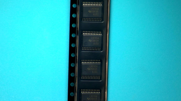
| SN74LVCC3245ADBR COUNTRY OF ORIGIN |
SN74LVCC3245ADBR PARAMETRIC INFO
|
SN74LVCC3245ADBR PACKAGE INFO
|
SN74LVCC3245ADBR MANUFACTURING INFO
|
SN74LVCC3245ADBR PACKAGING INFO
|
SN74LVCC3245ADBR EACD MODELS
|
| SN74LVCC3245ADBR APPLICATIONS |
|
| COUNTRY OF ORIGIN |
| Malaysia |
|
PARAMETRIC INFO
|
| Number of Channels |
8 |
| Channel Type |
Bidirectional |
| Logic Family |
LVC |
| Process Technology |
CMOS |
| Logic Function |
Voltage Level Translator |
| Output Type |
3-State |
| Minimum High Level Input Voltage (V) |
1.7 |
| Minimum Latch-Up Current (mA) |
250 |
| Minimum Operating Temperature (°C) |
-40 |
| Maximum Operating Temperature (°C) |
85 |
| Minimum Storage Temperature (°C) |
-65 |
| Maximum Storage Temperature (°C) |
150 |
| Minimum Operating Supply Voltage (V) |
2.3/3 |
| Maximum Operating Supply Voltage (V) |
3.6/5.5 |
| Typical Operating Supply Voltage (V) |
3.3/5 |
| Maximum High Level Output Current (mA) |
-twenty four |
| Maximum Low Level Output Current (mA) |
twenty four |
| Maximum Quiescent Current (mA) |
0.08 |
| Maximum Propagation Delay Time @ Maximum CL (ns) |
11.2@2.3V to 2.7V@3V to 3.6V |
| Absolute Propagation Delay Time (ns) |
14.5 |
|
|
PACKAGE INFO
|
| Supplier packaging |
SSOP |
| Basic package type |
Lead-Frame SMT |
| Number of pins |
twenty four |
| Pin shape |
Gull-wing |
| PCB |
twenty four |
| ears |
N/R |
| Pin spacing (mm) |
0.65 |
| Package length (mm) |
8.5(Max) |
| Package width (mm) |
5.6(Max) |
| Package height (mm) |
2(Max)-0.05(Min) |
| Package diameter (mm) |
N/R |
| Package Overall Length (mm) |
8.5(Max) |
| Package Overall Width (mm) |
8.2(Max) |
| Package Overall Height (mm) |
2(Max) |
| Mounting surface height (mm) |
2(Max) |
| Install |
Surface Mount |
| Package weight (g) |
not applicable |
| Packaging materials |
Plastic |
| package instruction |
Shrink Small Outline Package |
| Package series name |
SO |
| JEDEC |
MO-150 |
|
|
MANUFACTURING INFO
|
| MSL |
1 |
| Maximum reflow temperature (°C) |
260 |
| Reflow soldering time (seconds) |
30 |
| Number of reflow cycles |
3 |
| standard |
J-STD-020D |
| Reflow temperature source |
Link to datasheet |
| Maximum wave soldering temperature (°C) |
N/R |
| Wave soldering time (seconds) |
N/R |
| Lead Finish(Plating) |
Au |
| Plating materials |
Pd over Ni |
| Terminal Base Material |
Cu Alloy |
| Number of Wave Cycles |
N/R |
|
|
PACKAGING INFO
|
| Packaging Suffix |
R |
| Package |
Tape and reel packaging |
| Packing quantity |
2000 |
| Reel Diameter (in) |
13 |
| Reel Width (mm) |
16.4 |
| Tape Pitch (mm) |
12 |
| Tape Width (mm) |
16 |
| Component Orientation |
Q1 |
| packaging type file |
Link to datasheet |
|
|
ECAD MODELS
|
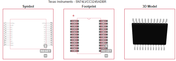
|
|
APPLICATIONS
|
• Level translation
|
| • USB |
| • Interfacing |
| • Analog and digital applications |
| |