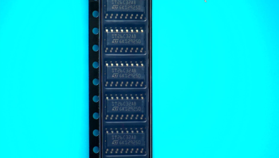
 |
|
| • CMOS design for low power |
| • ± 0.2 V sensitivity over input common mode
voltage range |
| • Typical propagation delay: 19 ns |
| • Typical input hysteresis: 60 mV |
| • Input will not load line when VCC = 0 V |
| • Meets the requirements of EIA standard
RS-422, RS-423 |
| • 3-state outputs for connection to system buses |
| • Available in surface mount |
|
| CATALOG |
| ST26C32ABDR COUNTRY OF ORIGIN |
| ST26C32ABDR PARAMETRIC INFO |
| ST26C32ABDR PACKAGE INFO |
| ST26C32ABDR MANUFACTURING INFO |
| ST26C32ABDR PACKAGING INFO |
| ST26C32ABDR ECAD MODELS |
|
| COUNTRY OF ORIGIN |
| China |
| Malaysia |
| Morocco |
| Philippines |
| Thailand |
| United States of America |
|
| PARAMETRIC INFO |
| Function |
Line Receiver |
| Number of Receivers |
4 |
| Data Transmission Topology |
Point-to-Point|Multidrop |
| Receiver Signal Type |
Single-Ended|Differential |
| Charge Pump |
No |
| Input Logic Level |
CMOS |
| Output Logic Level |
CMOS |
| Receiver Communication Type |
RS-422|RS-423 |
| Interface Standards |
EIA-422|EIA-423|RS-422|RS-423 |
| Number of Receiver Enables |
2 |
| Number of Receivers per Line |
10 |
| Data Rate |
20Mbps |
| Driving Mode |
3-State |
| Minimum Operating Temperature (°C) |
-40 |
| Maximum Operating Temperature (°C) |
85 |
| Maximum Storage Temperature (°C) |
150 |
| Minimum Storage Temperature (°C) |
-65 |
| Power Supply Type |
Single |
| Typical Single Supply Voltage (V) |
5 |
| Minimum Single Supply Voltage (V) |
4.5 |
| Maximum Single Supply Voltage (V) |
5.5 |
| Maximum Supply Current (mA) |
23 |
|
| |
| PACKAGE INFO |
| Supplier Package |
SO |
| Basic Package Type |
Lead-Frame SMT |
| Pin Count |
16 |
| Lead Shape |
Gull-wing |
| PCB |
16 |
| Tab |
N/R |
| Pin Pitch (mm) |
1.27 |
| Package Length (mm) |
10(Max) |
| Package Width (mm) |
4(Max) |
| Package Height (mm) |
1.65(Max) |
| Package Diameter (mm) |
N/R |
| Seated Plane Height (mm) |
1.75(Max) |
| Mounting |
Surface Mount |
| Package Material |
Plastic |
| Package Description |
Small Outline IC |
| Package Family Name |
SO |
| Jedec |
N/A |
|
| |
| MANUFACTURING INFO |
| MSL |
3 |
| Maximum Reflow Temperature (°C) |
260 |
| Reflow Solder Time (Sec) |
30 |
| Number of Reflow Cycle |
3 |
| Reflow Temp. Source |
Link to Datasheet |
| Maximum Wave Temperature (°C) |
N/R |
| Wave Solder Time (Sec) |
N/R |
| Lead Finish(Plating) |
Au |
| Under Plating Material |
Pd over Ni |
| Terminal Base Material |
Cu Alloy |
| Shelf Life Period |
2 Years |
|
| |
| PACKAGING INFO |
| Packaging Suffix |
R |
| Packaging |
Tape and Reel |
| Quantity Of Packaging |
2500 |
| Packaging Document |
Link to Datasheet |
|
| |
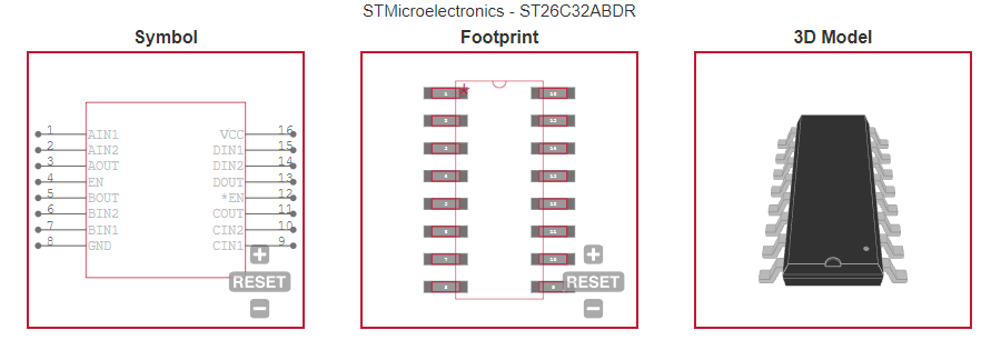
| ECAD MODELS |
 |
|

