 |
|
| • 1-to-8 Bidirectional translating switches |
| • I
2C Bus and SMBus compatible |
| • Active-low reset input |
| • Three address pins, allowing up to eight
TCA9548A devices on the I
2C bus
|
| • Channel selection through an I
2C Bus, in any
combination
|
| • Power up with all switch channels deselected |
| • Low RON switches |
| • Allows voltage-level translation between 1.8-V,
2.5-V, 3.3-V, and 5-V buses |
| • No glitch on power up |
| • Supports hot insertion |
| • Low standby current |
| • Operating power-supply voltage range of
1.65 V to 5.5 V |
| • 5-V Tolerant inputs
|
| • 0- to 400-kHz Clock frequency |
| • Latch-up performance exceeds 100 mA Per JESD
78, class II |
• ESD Protection exceeds JESD 22
– ±2000-V Human-body model (A114-A)
– 200-V Machine model (A115-A)
– ±1000-V Charged-device model (C101)
|
|
| CATALOG |
| TCA9548ARGER COUNTRY OF ORIGIN |
| TCA9548ARGER PARAMETRIC INFO |
| TCA9548ARGER PACKAGE INFO |
| TCA9548ARGER MANUFACTURING INFO |
| TCA9548ARGER PACKAGING INFO |
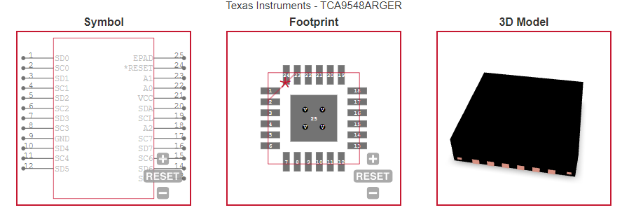
| TCA9548ARGER ECAD MODELS |
| TCA9548ARGER FUNCTIONAL BLOCK DIAGRAM |
| TCA9548ARGER APPLICATIONS |
|
| COUNTRY OF ORIGIN |
| Japan |
| Malaysia |
|
| PARAMETRIC INFO |
| Logic Function |
I2C Bus Switch |
| Number of Elements per Chip |
1 |
| Number of Inputs per Chip |
8 |
| Number of Outputs per Chip |
8 |
| Configuration |
8 x 1:1 |
| Maximum Supply Current (mA) |
100 |
| Maximum On Resistance (Ohm) |
25(Typ) |
| Minimum Operating Supply Voltage (V) |
1.65 |
| Maximum Operating Supply Voltage (V) |
5.5 |
| Typical Operating Supply Voltage (V) |
1.8|2.5|3.3|5 |
| Minimum Operating Temperature (°C) |
-40 |
| Maximum Operating Temperature (°C) |
85 |
| Minimum Storage Temperature (°C) |
-65 |
| Maximum Storage Temperature (°C) |
150 |
| Maximum Propagation Delay Time @ Maximum CL (ns) |
1@1.65V to 5.5V |
| Absolute Propagation Delay Time (ns) |
1 |
| Propagation Delay Test Condition (pF) |
50 |
| Maximum Low Level Output Current (mA) |
9(Typ) |
| Maximum Quiescent Current (uA) |
80 |
| Typical Quiescent Current (uA) |
50 |
|
|
| PACKAGE INFO |
| Supplier Package |
VQFN EP |
| Basic Package Type |
Non-Lead-Frame SMT |
| Pin Count |
24 |
| Lead Shape |
No Lead |
| PCB |
24 |
| Tab |
N/R |
| Pin Pitch (mm) |
0.5 |
| Package Length (mm) |
4.15(Max) |
| Package Width (mm) |
4.15(Max) |
| Package Height (mm) |
0.95(Max) |
| Package Diameter (mm) |
N/R |
| Package Overall Length (mm) |
4.15(Max) |
| Package Overall Width (mm) |
4.15(Max) |
| Package Overall Height (mm) |
1(Max) |
| Seated Plane Height (mm) |
1(Max) |
| Mounting |
Surface Mount |
| Package Weight (g) |
N/A |
| Package Material |
Plastic |
| Package Description |
Very Thin Quad Flat No Lead Package, Exposed Pad |
| Package Family Name |
QFN |
| Jedec |
MO-220 |
|
|
| MANUFACTURING INFO |
| MSL |
2 |
| Maximum Reflow Temperature (°C) |
260 |
| Reflow Solder Time (Sec) |
30 |
| Number of Reflow Cycle |
3 |
| Standard |
J-STD-020D |
| Reflow Temp. Source |
Link to Datasheet |
| Maximum Wave Temperature (°C) |
N/R |
| Wave Solder Time (Sec) |
N/R |
| Lead Finish(Plating) |
Au |
| Under Plating Material |
Pd over Ni |
| Terminal Base Material |
Cu Alloy |
| Number of Wave Cycles |
N/R |
|
|
| PACKAGING INFO |
| Packaging Suffix |
R |
| Packaging |
Tape and Reel |
| Quantity Of Packaging |
3000 |
| Reel Diameter (in) |
13 |
| Reel Width (mm) |
12.4 |
| Tape Pitch (mm) |
8 |
| Tape Width (mm) |
12 |
| Component Orientation |
Q2 |
| Packaging Document |
Link to Datasheet |
|
|
| ECAD MODELS |
 |
|
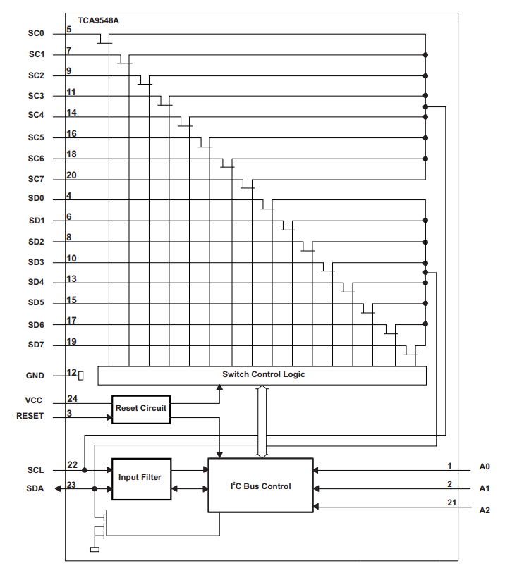
| FUNCTIONAL BLOCK DIAGRAM |
 |
|
| APPLICATIONS |
| • Servers |
| • Routers (telecom switching equipment) |
| • Factory Automation |
| • Products with I
2C slave address conflicts (such as
multiple, identical temperature sensors)
|
| |
| |