|
|
• Fully Differential Amplifier (FDA) Architecture
|
• Bandwidth: 500 MHz (G = 2 V/V)
|
• Gain Bandwidth Product: 850 MHz
|
• Slew Rate: 1500 V/µs
|
• HD2
: –95 dBc at 10 MHz (2 VPP, RL = 500 Ω)
|
• HD3
: –90 dBc at 10 MHz (2 VPP, RL = 500 Ω)
|
• Input Voltage Noise: 2.2 nV/Hz (f > 100 kHz)
|
• Low offset drift: ±0.5 µV/°C (typ)
|
• Negative Rail Input (NRI)
|
• Rail-to-Rail Output (RRO)
|
• Robust Operation for Rload ≥ 50 Ω
|
• Output Common-Mode Control
|
• Power-Down Capability: 2 µA (typ)
|
|
| CATALOG |
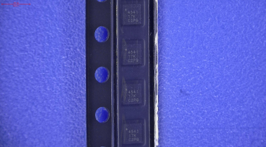
THS4541IRUNR COUNTRY OF ORIGIN
|
THS4541IRUNR PARAMETRIC INFO
|
THS4541IRUNR PACKAGE INFO
|
THS4541IRUNR MANUFACTURING INFO
|
THS4541IRUNR PACKAGING INFO
|
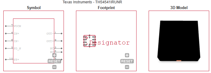
THS4541IRUNR ECAD MODELS
|
THS4541IRUNR APPLICATIONS
|
|
COUNTRY OF ORIGIN
|
Malaysia
|
|
PARAMETRIC INFO
|
| Type |
Differential Amplifier |
| Rail to Rail |
Rail to Rail Output |
| Number of Elements per Chip |
1 |
| Number of Channels per Chip |
1 |
| Minimum PSRR (dB) |
85 |
| Typical Gain Bandwidth Product (MHz) |
850 |
| Maximum Input Offset Voltage (mV) |
0.45@5V |
| Maximum Input Bias Current (uA) |
13@5V |
| Minimum CMRR (dB) |
85 |
| Maximum Quiescent Current (mA) |
10.5@5V |
| Minimum CMRR Range (dB) |
85 to 95 |
| Typical Output Current (mA) |
100@5V |
| Maximum Input Resistance (MOhm) |
0.11(Typ)@5V |
| Typical Slew Rate (V/us) |
1500@5V |
| Typical Input Offset Current (uA) |
0.15@5V |
| Maximum Input Offset Current (uA) |
0.5@5V |
| Maximum Voltage Gain Range (dB) |
100 to 125 |
| Maximum Voltage Gain (dB) |
119(Typ) |
| Minimum Operating Temperature (°C) |
-40 |
| Maximum Operating Temperature (°C) |
125 |
| Minimum Storage Temperature (°C) |
-65 |
| Maximum Storage Temperature (°C) |
150 |
| Power Supply Type |
Single|Dual |
| Maximum Supply Voltage Range (V) |
5 to 7 |
| Minimum Single Supply Voltage (V) |
2.7 |
| Typical Single Supply Voltage (V) |
5 |
| Maximum Single Supply Voltage (V) |
5.4 |
| Minimum Dual Supply Voltage (V) |
±1.35 |
| Typical Dual Supply Voltage (V) |
±2.5 |
| Maximum Dual Supply Voltage (V) |
±2.7 |
| Maximum Operating Supply Voltage (V) |
±2.7|5.4 |
|
|
PACKAGE INFO
|
| Supplier Package |
WQFN |
| Basic Package Type |
Non-Lead-Frame SMT |
| Pin Count |
10 |
| Lead Shape |
No Lead |
| PCB |
10 |
| Tab |
N/R |
| Pin Pitch (mm) |
0.5 |
| Package Length (mm) |
2.1(Max) |
| Package Width (mm) |
2.1(Max) |
| Package Height (mm) |
0.75(Max) |
| Package Diameter (mm) |
N/R |
| Package Overall Length (mm) |
2.1(Max) |
| Package Overall Width (mm) |
2.1(Max) |
| Package Overall Height (mm) |
0.8(Max) |
| Seated Plane Height (mm) |
0.8(Max) |
| Mounting |
Surface Mount |
| Package Material |
Plastic |
| Package Family Name |
QFN |
| Jedec |
N/A |
|
|
MANUFACTURING INFO
|
| MSL |
2 |
| Maximum Reflow Temperature (°C) |
260 |
| Reflow Solder Time (Sec) |
30 |
| Number of Reflow Cycle |
3 |
| Standard |
J-STD-020D |
| Reflow Temp. Source |
Link to Datasheet |
| Maximum Wave Temperature (°C) |
N/R |
| Wave Solder Time (Sec) |
N/R |
| Lead Finish(Plating) |
Au |
| Under Plating Material |
Pd over Ni |
| Terminal Base Material |
Cu Alloy |
|
|
PACKAGING INFO
|
| Packaging Suffix |
R |
| Packaging |
Tape and Reel |
| Quantity Of Packaging |
3000 |
| Packaging Document |
Link to Datasheet |
|
|
ECAD MODELS
|
|
|
APPLICATIONS
|
• Low-Power, High-Performance ADC Driver– SAR, ΔΣ, and Pipeline
|
| • Low Power, High Performance(DC or AC Coupled)– Single-Ended to Differential Amplifier– Differential to Differential Amplifier |
| • Differential Active Filters |
• Differential Transimpedance for DAC Outputs
|
• DC- or AC-Coupled Interface to the ADC3xxx
Family of Low-Power, High-Performance ADCs
|
| • Pin-Compatible to ADA4932-1 (VQFN-16) |
| |