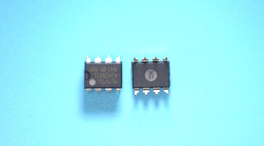
TL082ACN STMicroelectronics IC OPAMP JFET 4MHZ 8DIP

label:
2024/11/12 116
TL082ACN STMicroelectronics IC OPAMP JFET 4MHZ 8DIP


• Wide common-mode (up to VCC+) and differential voltage range
• Low input bias and offset current
• Output short-circuit protection
• High input impedance JFET input stage
• Internal frequency compensation 
• Latch up free operation
• High slew rate: 16 V/µs (typical)


CATALOG
TL082ACN COUNTRY OF ORIGIN
TL082ACN PARAMETRIC INFO
TL082ACN PACKAGE INFO
TL082ACN MANUFACTURING INFO
TL082ACN PACKAGING INFO
TL082ACN ECAD MODELS


COUNTRY OF ORIGIN
China


PARAMETRIC INFO
Manufacturer Type General Purpose Amplifier
Type General Purpose Amplifier
Number of Channels per Chip 2
Process Technology BiFET
Typical Gain Bandwidth Product (MHz) 4
Minimum Dual Supply Voltage (V) ±3
Maximum Input Offset Voltage (mV) 6@±15V
Typical Dual Supply Voltage (V) ±5|±9|±12|±15
Maximum Dual Supply Voltage (V) ±18
Maximum Input Offset Current (uA) 0.0001@±15V
Maximum Input Bias Current (uA) 0.0002@±15V
Maximum Operating Supply Voltage (V) ±18
Maximum Supply Voltage Range (V) 36 to 37
Minimum CMRR (dB) 80
Minimum CMRR Range (dB) 80 to 85
Typical Voltage Gain (dB) 106.02
Typical Slew Rate (V/us) 16@±15V
Typical Input Noise Voltage Density (nV/rtHz) 15@±15V
Shut Down Support No
Minimum Operating Temperature (°C) 0
Maximum Operating Temperature (°C) 70
Power Supply Type Dual
Maximum Supply Current (mA) 2.5@±15V
Maximum Power Dissipation (mW) 680


PACKAGE INFO
Supplier Package PDIP
Basic Package Type Through Hole
Pin Count 8
Lead Shape Through Hole
PCB 8
Tab N/R
Pin Pitch (mm) 2.54
Package Length (mm) 9.27
Package Width (mm) 6.35
Package Height (mm) 3.3
Package Diameter (mm) N/R
Seated Plane Height (mm) 5.33(Max)
Mounting Through Hole
Package Material Plastic
Package Description Plastic Dual In Line Package
Package Family Name DIP
Jedec MS-001BA
Package Outline Link to Datasheet


MANUFACTURING INFO
MSL N/R
Maximum Reflow Temperature (°C) N/A
Reflow Solder Time (Sec) N/A
Number of Reflow Cycle N/A
Standard IPC-1752
Reflow Temp. Source Link to Datasheet
Maximum Wave Temperature (°C) 260
Wave Solder Time (Sec) 10
Wave Temp. Source Link to Datasheet
Lead Finish(Plating) Matte Sn annealed
Under Plating Material Ag
Terminal Base Material Cu Alloy
Shelf Life Period 2 Years
Number of Wave Cycles 2


PACKAGING INFO
Packaging Tube
Quantity Of Packaging 50
Packaging Document Link to Datasheet


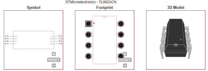
ECAD MODELS

Продукт RFQ