|
|
• High slew rate: 20 V/μs (TL08xH, typ)
|
• Low offset voltage: 1 mV (TL08xH, typ)
|
• Low offset voltage drift: 2 μV/°C
|
| • Low power consumption: 940 μA/ch (TL08xH, typ) |
| • Wide common-mode and differential
voltage ranges
– Common-mode input voltage range
includes VCC+ |
| • Low input bias and offset currents |
| • Low noise:
Vn = 18 nV/√Hz (typ) at f = 1 kHz
|
| • Output short-circuit protection
|
| • Low total harmonic distortion: 0.003% (typ) |
| • Wide supply voltage:
±2.25 V to ±20 V, 4.5 V to 40 V |
|
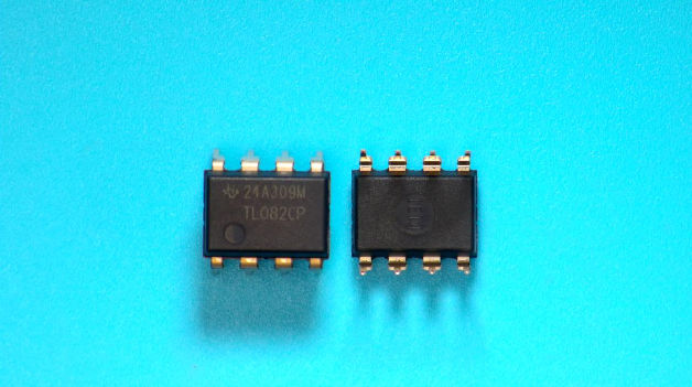
| CATALOG |
| TL082CP COUNTRY OF ORIGIN |
TL082CP PARAMETRIC INFO
|
TL082CP PACKAGE INFO
|
TL082CP MANUFACTURING INFO
|
TL082CP PACKAGING INFO
|
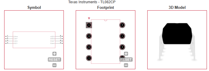
TL082CP ECAD MODELS
|
TL082CP APPLICATIONS
|
|
| COUNTRY OF ORIGIN |
| Taiwan (Province of China) |
| Mexico |
|
PARAMETRIC INFO
|
| Manufacturer Type |
General Purpose Amplifier |
| Type |
General Purpose Amplifier |
| Minimum Single Supply Voltage (V) |
4.5 |
| Number of Channels per Chip |
2 |
| Typical Single Supply Voltage (V) |
5|9|12|15|18|24|28 |
| Maximum Single Supply Voltage (V) |
40 |
| Maximum Quiescent Current (mA) |
5.6@±15V |
| Minimum Dual Supply Voltage (V) |
±2.25 |
| Typical Gain Bandwidth Product (MHz) |
3 |
| Maximum Input Offset Voltage (mV) |
15@±15V |
| Typical Dual Supply Voltage (V) |
±3|±5|±9|±12|±15|±18 |
| Maximum Input Offset Current (uA) |
0.0002@±15V |
| Maximum Dual Supply Voltage (V) |
±20 |
| Maximum Operating Supply Voltage (V) |
±20|40 |
| Maximum Input Bias Current (uA) |
0.0004@±15V |
| Minimum CMRR (dB) |
70 |
| Maximum Supply Voltage Range (V) |
37 to 44 |
| Minimum CMRR Range (dB) |
70 to 71 |
| Typical Voltage Gain (dB) |
106.02 |
| Typical Slew Rate (V/us) |
13@±15V |
| Typical Input Noise Voltage Density (nV/rtHz) |
18@±15V |
| Typical Noninverting Input Current Noise Density (pA/rtHz) |
0.01@±15V |
| Shut Down Support |
No |
| Minimum Operating Temperature (°C) |
0 |
| Maximum Operating Temperature (°C) |
70 |
| Power Supply Type |
Single|Dual |
|
|
PACKAGE INFO
|
| Supplier Package |
PDIP |
| Basic Package Type |
Through Hole |
| Pin Count |
8 |
| Lead Shape |
Through Hole |
| PCB |
8 |
| Tab |
N/R |
| Pin Pitch (mm) |
2.54 |
| Package Length (mm) |
10.16(Max) |
| Package Width (mm) |
6.6(Max) |
| Package Height (mm) |
5.08(Max) - 0.51(Min) |
| Package Diameter (mm) |
N/R |
| Package Overall Length (mm) |
10.16(Max) |
| Package Overall Width (mm) |
10.92(Max) |
| Package Overall Height (mm) |
5.08(Max) |
| Seated Plane Height (mm) |
5.08(Max) |
| Mounting |
Through Hole |
| Package Weight (g) |
N/A |
| Package Material |
Plastic |
| Package Description |
Plastic Dual In Line Package |
| Package Family Name |
DIP |
| Jedec |
MS-001BA |
| Package Outline |
Link to Datasheet |
|
|
MANUFACTURING INFO
|
| MSL |
N/R |
| Maximum Reflow Temperature (°C) |
N/R |
| Reflow Solder Time (Sec) |
N/R |
| Reflow Temp. Source |
Link to Datasheet |
| Maximum Wave Temperature (°C) |
N/A |
| Wave Solder Time (Sec) |
N/A |
| Lead Finish(Plating) |
Au |
| Under Plating Material |
Pd over Ni |
| Terminal Base Material |
Cu Alloy |
|
|
PACKAGING INFO
|
| Packaging |
Tube |
| Quantity Of Packaging |
50 |
| Packaging Document |
Link to Datasheet |
|
|
ECAD MODELS
|
|
|
APPLICATIONS
|
• Solar energy: string and central inverter
|
• Motor drives: AC and servo drive control and
power stage modules
|
| • Single phase online UPS
|
| • Three phase UPS
|
| • Pro audio mixers |
| • Battery test equipment |
|
| |