TL084CDR Texas Instruments IC OPAMP JFET 3MHZ 14SOIC

label:
2024/01/22 230


• High slew rate: 20 V/μs (TL08xH, typ)  
• Low offset voltage: 1 mV (TL08xH, typ)  
• Low offset voltage drift: 2 μV/°C
• Low power consumption: 940 μA/ch (TL08xH, typ)  
• Wide common-mode and differential voltage ranges
   – Common-mode input voltage range includes VCC+
• Low input bias and offset currents
• Low noise: Vn = 18 nV/√Hz (typ) at f = 1 kHz
• Output short-circuit protection
• Low total harmonic distortion: 0.003% (typ)  
• Wide supply voltage: ±2.25 V to ±20 V, 4.5 V to 40 V


CATALOG
TL084CDR COUNTRY OF ORIGIN
TL084CDR PARAMETRIC INFO
TL084CDR PACKAGE INFO
TL084CDR MANUFACTURING INFO  
TL084CDR PACKAGING INFO
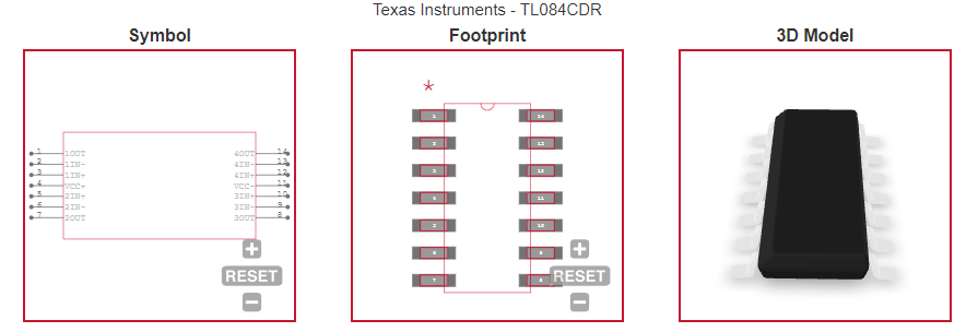
TL084CDR ECAD MODELS
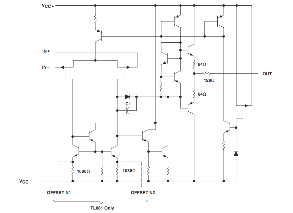
TL084CDR FUNCTIONAL BLOCK DIAGRAM
TL084CDR APPLICATIONS


COUNTRY OF ORIGIN
Mexico
Taiwan (Province of China)
Malaysia
China


PARAMETRIC INFO
Manufacturer Type General Purpose Amplifier
Type General Purpose Amplifier
Minimum Single Supply Voltage (V) 10
Number of Channels per Chip 4
Typical Single Supply Voltage (V) 12|15|18|24|28
Typical Input Resistance (Ohm) 1T
Maximum Single Supply Voltage (V) 30
Maximum Quiescent Current (mA) 11.2@±15V
Minimum Dual Supply Voltage (V) ±5
Typical Gain Bandwidth Product (MHz) 3
Maximum Input Offset Voltage (mV) 15@±15V
Typical Dual Supply Voltage (V) ±9|±12
Maximum Input Offset Current (uA) 0.0002@±15V
Maximum Dual Supply Voltage (V) ±15
Maximum Input Voltage Range (V) -15 to 15
Maximum Operating Supply Voltage (V) ±15|30
Maximum Input Bias Current (uA) 0.0004@±15V
Minimum CMRR (dB) 70
Maximum Supply Voltage Range (V) 30 to 32
Minimum CMRR Range (dB) 70 to 71
Typical Voltage Gain (dB) 106.02
Typical Slew Rate (V/us) 13@±15V
Minimum Slew Rate (V/us) 8@±15V
Typical Input Offset Current (uA) 0.000005@±15V
Typical Output Current (mA) 10
Typical Input Noise Voltage Density (nV/rtHz) 18@±15V
Typical Noninverting Input Current Noise Density (pA/rtHz) 0.01@±15V
Typical Input Bias Current (uA) 0.00003@±15V
Shut Down Support No
Minimum Operating Temperature (°C) 0
Maximum Operating Temperature (°C) 70
Minimum Storage Temperature (°C) -65
Maximum Storage Temperature (°C) 150
Power Supply Type Single|Dual
Maximum Power Dissipation (mW) 680
Input Offset Voltage Drift (uV/°C) 18(Typ)


PACKAGE INFO
Supplier Package SOIC
Basic Package Type Lead-Frame SMT
Pin Count 14
Lead Shape Gull-wing
PCB 14
Tab N/R
Pin Pitch (mm) 1.27
Package Length (mm) 8.75(Max)
Package Width (mm) 4(Max)
Package Height (mm) 1.5(Max)
Package Diameter (mm) N/R
Package Overall Length (mm) 8.75(Max)
Package Overall Width (mm) 6.2(Max)
Package Overall Height (mm) 1.75(Max)
Seated Plane Height (mm) 1.75(Max)
Mounting Surface Mount
Package Weight (g) N/A
Package Material Plastic
Package Description Small Outline IC
Package Family Name SO
Jedec MS-012AB
Package Outline Link to Datasheet


MANUFACTURING INFO
MSL 1
Maximum Reflow Temperature (°C) 260
Reflow Solder Time (Sec) 30
Number of Reflow Cycle 3
Standard J-STD-020D
Reflow Temp. Source Link to Datasheet
Maximum Wave Temperature (°C) N/R
Wave Solder Time (Sec) N/R
Lead Finish(Plating) Au
Under Plating Material Pd over Ni
Terminal Base Material Cu Alloy


PACKAGING INFO
Packaging Suffix R
Packaging Tape and Reel
Quantity Of Packaging 2500
Reel Diameter (in) 13
Reel Width (mm) 16.4
Tape Pitch (mm) 8
Tape Width (mm) 16
Component Orientation Q1
Packaging Document Link to Datasheet


ECAD MODELS


FUNCTIONAL BLOCK DIAGRAM


APPLICATIONS
• Solar energy: string and central inverter
• Motor drives: AC and servo drive control and power stage modules
• Single phase online UPS
• Three phase UPS
• Pro audio mixers
• Battery test equipment


Продукт RFQ