| Rail to Rail |
Rail to Rail Output |
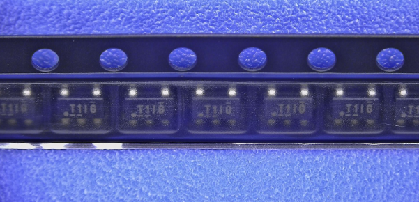
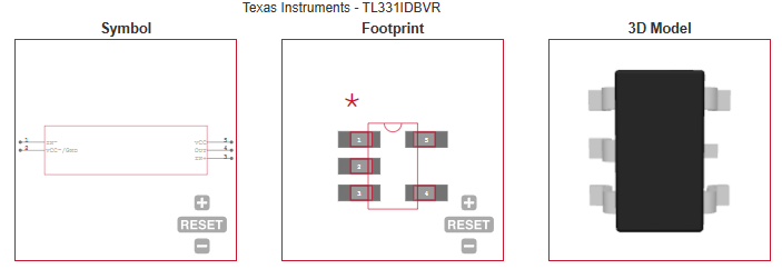
| Manufacturer Type |
Differential Comparator |
| Number of Channels per Chip |
1 |
| Output Type |
Open Collector |
| Maximum Input Offset Voltage (mV) |
5@30V |
| Maximum Input Bias Current (uA) |
0.25@5V |
| Maximum Input Voltage Range (V) |
-0.3 to 36 |
| Typical Voltage Gain (dB) |
106.02 |
| Typical Voltage Gain Range (dB) |
90 to 110 |
| Strobe Capability |
No |
| Typical Output Current (mA) |
20(Max) |
| Typical Input Offset Current (uA) |
0.005@5V |
| Maximum Input Offset Current (uA) |
0.05@5V |
| Typical Response Time (us) |
1.3 |
| Typical Response Time Range (us) |
0.5 to 5 |
| Maximum Propagation Delay Time (ns) |
1300(Typ) |
| Minimum Operating Temperature (°C) |
-40 |
| Maximum Operating Temperature (°C) |
85 |
| Minimum Storage Temperature (°C) |
-65 |
| Maximum Storage Temperature (°C) |
150 |
| Power Supply Type |
Single|Dual |
| Integrated Voltage Reference |
No |
| Maximum Test Temperature (°C) |
85 |
| Minimum Test Temperature (°C) |
-40 |
| Maximum Operating Supply Voltage (V) |
±18|36 |
| Integrated OP Amp |
No |
| Minimum Single Supply Voltage (V) |
2 |
| Typical Single Supply Voltage (V) |
3|5|9|12|15|18|24|28 |
| Maximum Single Supply Voltage (V) |
36 |
| Minimum Dual Supply Voltage (V) |
±1 |
| Typical Dual Supply Voltage (V) |
±3|±5|±9|±12|±15 |
| Maximum Dual Supply Voltage (V) |
±18 |
| Maximum Quiescent Current (mA) |
0.7@5V |