 |
|
| • Output Voltage 5 V ± 2 % up to Output Currents of 50 mA |
| • Output Voltage 5 V ± 3 % up to Output Currents 100 mA |
| • Very Low Dropout Voltage |
| • Very Low Current Consumption: typ. 40 µA |
| • Enable Input |
| • Output Current Limitation |
| • Reverse Polarity Protection |
| • Overtemperature Shutdown |
| • Wide Temperature Range From -40 °C up to 150 °C |
| • Suitable for Use in Automotive Electronics |
| • Green Product (RoHS compliant) |
| • AEC Qualified |
|
| CATALOG |
| TLE42664G COUNTRY OF ORIGIN |
| TLE42664G LIFECYCLE |
| TLE42664G PARAMETRIC INFO |
| TLE42664G PACKAGE INFO |
| TLE42664G MANUFACTURING INFO |
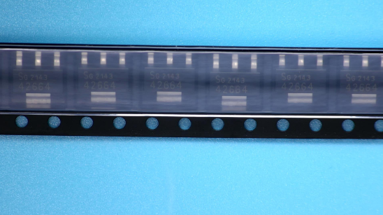
| TLE42664G PACKAGING INFO |
| TLE42664G FUNCTIONAL BLOCK DIAGRAM |
|
| COUNTRY OF ORIGIN |
| Malaysia |
|
| LIFECYCLE |
| Unconfirmed |
|
| PARAMETRIC INFO |
| Type |
LDO |
| Number of Outputs |
1 |
| Maximum Output Current (A) |
0.1 |
| Minimum Operating Temperature (°C) |
-40 |
| Maximum Operating Temperature (°C) |
150 |
| Output Voltage Range (V) |
1.8 to 10 |
| Output Type |
Fixed |
| Junction to Ambient |
139K/W(Typ) |
| Junction to Case |
17K/W(Typ) |
| Polarity |
Positive |
| Special Features |
Current Limit|Reverse Polarity Protection|Thermal Shutdown Protection |
| Load Regulation |
90mV |
| Line Regulation |
30mV |
| Maximum Quiescent Current (mA) |
0.07 |
| Maximum Dropout Voltage @ Current (V) |
0.5@100mA |
| Minimum Input Voltage (V) |
5.5 |
| Maximum Input Voltage (V) |
40 |
| Output Voltage (V) |
5 |
| Typical Quiescent Current (mA) |
0.04 |
| Typical Dropout Voltage @ Current (V) |
0.25@100mA |
| Accuracy (%) |
±3 |
| Minimum Storage Temperature (°C) |
-50 |
| Maximum Storage Temperature (°C) |
150 |
|
| |
| PACKAGE INFO |
| Supplier Package |
SOT-223 |
| Basic Package Type |
Lead-Frame SMT |
| Pin Count |
4 |
| Lead Shape |
Gull-wing |
| PCB |
3 |
| Tab |
Tab |
| Pin Pitch (mm) |
2.3 |
| Package Length (mm) |
6.5 |
| Package Width (mm) |
3.5 |
| Package Height (mm) |
1.6 |
| Package Diameter (mm) |
N/R |
| Package Overall Length (mm) |
6.5 |
| Package Overall Width (mm) |
7 |
| Package Overall Height (mm) |
1.8(Max) |
| Seated Plane Height (mm) |
1.8(Max) |
| Mounting |
Surface Mount |
| Package Material |
Plastic |
| Package Description |
Small Outline Transistor |
| Package Family Name |
SOT |
| Jedec |
TO-261AA |
| Package Outline |
Link to Datasheet |
|
| |
| MANUFACTURING INFO |
| MSL |
1 |
| Maximum Reflow Temperature (°C) |
260 |
| Reflow Solder Time (Sec) |
30 |
| Number of Reflow Cycle |
3 |
| Standard |
J-STD-020D |
| Maximum Wave Temperature (°C) |
N/R |
| Wave Solder Time (Sec) |
N/R |
| Lead Finish(Plating) |
Matte Sn annealed |
| Under Plating Material |
Ag |
| Terminal Base Material |
Cu Alloy |
|
| |
| PACKAGING INFO |
| Packaging |
Tape and Reel |
| Quantity Of Packaging |
4000 |
| Packaging Document |
Link to Datasheet |
|
| |
| FUNCTIONAL BLOCK DIAGRAM |
 |
|