TLV271CDBVR Texas Instruments TLV27x Family of 550-µA/Ch, 3-MHz, Rail-to-Rail Output Operational Amplifiers

label:
2024/08/13 201
TLV271CDBVR Texas Instruments TLV27x Family of 550-µA/Ch, 3-MHz, Rail-to-Rail Output Operational Amplifiers


• Rail-to-Rail Output
• Wide Bandwidth: 3 MHz
• High Slew Rate: 2.4 V/µs
• Supply Voltage Range: 2.7 V to 16 V
• Supply Current: 550 µA/Channel
• Input Noise Voltage: 39 nV/√Hz
• Input Bias Current: 1 pA
• Specified Temperature Range:– Commercial Grade: 0°C to 70°C– Industrial Grade: −40°C to 125°C
• Ultrasmall Packaging:– 5-Pin SOT-23 (TLV271)– 8-Pin MSOP (TLV272)
• Ideal Upgrade for TLC72x Family


CATALOG
TLV271CDBVR COUNTRY OF ORIGIN
TLV271CDBVR PARAMETRIC INFO
TLV271CDBVR PACKAGE INFO
TLV271CDBVR MANUFACTURING INFO
TLV271CDBVR PACKAGING INFO
TLV271CDBVR ECAD MODELS
TLV271CDBVR APPLICATIONS


COUNTRY OF ORIGIN
Thailand
Taiwan (Province of China)
Malaysia
Philippines
China


PARAMETRIC INFO
Manufacturer Type Low Power Amplifier
Type Low Power Amplifier
Rail to Rail Rail to Rail Output
Minimum Single Supply Voltage (V) 2.7
Number of Channels per Chip 1
Process Technology CMOS
Minimum PSRR (dB) 70
Typical Single Supply Voltage (V) 5
Maximum Single Supply Voltage (V) 16
Output Type CMOS
Minimum Dual Supply Voltage (V) ±1.35
Typical Gain Bandwidth Product (MHz) 3
Maximum Input Offset Voltage (mV) 5@5V
Typical Dual Supply Voltage (V) ±5
Maximum Input Offset Current (uA) 0.00006@5V
Maximum Dual Supply Voltage (V) ±8
Maximum Operating Supply Voltage (V) ±8|16
Maximum Input Bias Current (uA) 0.00006@5V
Minimum CMRR (dB) 65
Maximum Supply Voltage Range (V) 16 to 17
Minimum CMRR Range (dB) 65 to 70
Typical Voltage Gain (dB) 110
Typical Slew Rate (V/us) 2.4@5V
Typical Settling Time (ns) 2900
Typical Output Current (mA) 7@5V
Typical Input Noise Voltage Density (nV/rtHz) 39@5V
Typical Noninverting Input Current Noise Density (pA/rtHz) 0.0006@5V
Shut Down Support No
Minimum Operating Temperature (°C) 0
Maximum Operating Temperature (°C) 70
Supplier Temperature Grade Commercial
Power Supply Type Single|Dual
Maximum Supply Current (mA) 0.66@5V
Maximum Power Dissipation (mW) 201


PACKAGE INFO
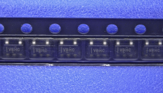
Supplier Package SOT-23
Basic Package Type Lead-Frame SMT
Pin Count 5
Lead Shape Gull-wing
PCB 5
Tab N/R
Pin Pitch (mm) 0.95
Package Length (mm) 3.05(Max)
Package Width (mm) 1.75(Max)
Package Height (mm) 1.1
Package Diameter (mm) N/R
Package Overall Length (mm) 3.05(Max)
Package Overall Width (mm) 3(Max)
Package Overall Height (mm) 1.45(Max)
Seated Plane Height (mm) 1.45(Max)
Mounting Surface Mount
Package Weight (g) N/A
Package Material Plastic
Package Description Small Outline Transistor
Package Family Name SOT
Jedec MO-178
Package Outline Link to Datasheet


MANUFACTURING INFO
MSL 1
Maximum Reflow Temperature (°C) 260
Reflow Solder Time (Sec) 30
Number of Reflow Cycle 3
Standard J-STD-020D
Reflow Temp. Source Link to Datasheet
Maximum Wave Temperature (°C) N/R
Wave Solder Time (Sec) N/R
Lead Finish(Plating) Matte Sn|Au
Under Plating Material N/A|Pd over Ni
Terminal Base Material Cu Alloy


PACKAGING INFO
Packaging Suffix R
Packaging Tape and Reel
Quantity Of Packaging 3000
Reel Diameter (in) 7
Reel Width (mm) 9
Tape Pitch (mm) 4
Tape Width (mm) 8
Component Orientation Q3
Packaging Document Link to Datasheet


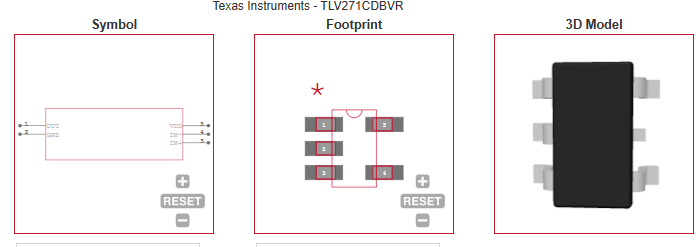
ECAD MODELS


APPLICATIONS
• E-Bike
• Power Banks
• Smoke detectors
• Solar Inverters
• Low-Power Motor Controls
• Battery-Powered Instruments
• Building Automation
Продукт RFQ