|
| |
• Low-voltage operation, VREF = 1.24V
|
• Adjustable output voltage, VO = VREF to 6V
|
• Reference voltage tolerances at 25°C– 0.5% for TLV431B– 1% for TLV431A– 1.5% for TLV431
|
| • Typical temperature drift– 4mV (0°C to 70°C)– 6mV (–40°C to 85°C)– 11mV (–40°C to 125°C)
|
| • Low operational cathode current, 80µA typical |
| • 0.25Ω typical output impedance |
| • Ultra-small SC-70 package offers 40% smaller footprint than SOT-23-3 |
• See TLVH431 and TLVH432 for:– Wider VKA (1.24V to 18 V) and IK (80mA)– Additional SOT-89 package– Multiple pinouts for SOT-23-3 and SOT-89
packages |
• On products compliant to MIL-PRF-38535, all parameters are tested unless otherwise noted. on all other products, production processing does not
necessarily include testing of all parameters. |
| |
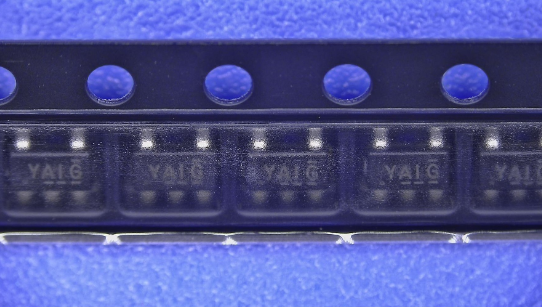
| CATALOG |
| TLV431AIDBVR COUNTRY OF ORIGIN |
TLV431AIDBVR PARAMETRIC INFO
|
TLV431AIDBVR PACKAGE INFO
|
TLV431AIDBVR MANUFACTURING INFO
|
TLV431AIDBVR PACKAGING INFO
|
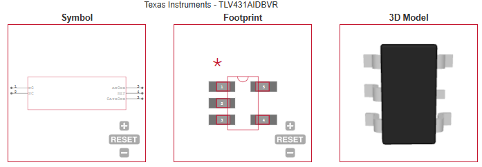
TLV431AIDBVR EACD MODELS
|
| TLV431AIDBVR APPLICATIONS |
|
| COUNTRY OF ORIGIN |
| Philippines |
| Malaysia |
| Thailand |
| China |
|
PARAMETRIC INFO
|
| Topology |
Shunt |
| Reference Type |
Adjustable |
| Output Voltage (V) |
1.24 to 6 |
| Initial Accuracy |
1% |
| Minimum Operating Temperature (°C) |
-40 |
| Maximum Operating Temperature (°C) |
85 |
| Maximum Storage Temperature (°C) |
150 |
| Minimum Storage Temperature (°C) |
-65 |
| Maximum Input Voltage (V) |
7 |
| Maximum Output Current (mA) |
15 |
| Maximum Temperature Coefficient |
138ppm/°C |
|
|
PACKAGE INFO
|
| Supplier Package |
SOT-23 |
| Basic Package Type |
Lead-Frame SMT |
| Pin Count |
5 |
| Lead Shape |
Gull-wing |
| PCB |
5 |
| Tab |
N/R |
| Pin Pitch (mm) |
0.95 |
| Package Length (mm) |
3.05(Max) |
| Package Width (mm) |
1.75(Max) |
| Package Height (mm) |
1.1 |
| Package Diameter (mm) |
N/R |
| Package Overall Length (mm) |
3.05(Max) |
| Package Overall Width (mm) |
3(Max) |
| Package Overall Height (mm) |
1.45(Max) |
| Seated Plane Height (mm) |
1.45(Max) |
| Mounting |
Surface Mount |
| Package Weight (g) |
N/A |
| Package Material |
Plastic |
| Package Description |
Small Outline Transistor |
| Package Family Name |
SOT |
| Jedec |
MO-178AA |
| Package Outline |
Link to Datasheet |
|
|
MANUFACTURING INFO
|
| MSL |
1 |
| Maximum Reflow Temperature (°C) |
260 |
| Reflow Solder Time (Sec) |
30 |
| Number of Reflow Cycle |
3 |
| Standard |
J-STD-020D |
| Reflow Temp. Source |
Link to Datasheet |
| Maximum Wave Temperature (°C) |
N/R |
| Wave Solder Time (Sec) |
N/R |
| Lead Finish(Plating) |
Matte Sn|Au |
| Under Plating Material |
N/A|Pd over Ni |
| Terminal Base Material |
Cu Alloy |
| Number of Wave Cycles |
N/R |
|
|
PACKAGING INFO
|
| Packaging Suffix |
R |
| Packaging |
Tape and Reel |
| Quantity Of Packaging |
3000 |
| Reel Diameter (in) |
7 |
| Tape Pitch (mm) |
4 |
| Tape Width (mm) |
8 |
| Component Orientation |
Q3 |
| Packaging Document |
Link to Datasheet |
|
|
ECAD MODELS
|
|
|
| APPLICATIONS |
| • Adjustable voltage and current referencing |
| • Secondary side regulation in flyback SMPSs |
| • Zener replacement |
| • Voltage monitoring |
• Comparator with integrated reference
|
| |