|
|
• Qualified for Automotive Applications
|
• 2% Accuracy Over Temperature
|
• Low IQ of 35 μA per Regulator
|
• Multiple Fixed-Output Voltage Combinations Possible from 1.2 V to 4.8 V
|
• High PSRR: 70 dB at 1kHz
|
• Stable With Effective Capacitance of 0.1 μF
|
|
| CATALOG |
TLV7103318QDSERQ1 COUNTRY OF ORIGIN
|
TLV7103318QDSERQ1 PARAMETRIC INFO
|
TLV7103318QDSERQ1 PACKAGE INFO
|
TLV7103318QDSERQ1 MANUFACTURING INFO
|
TLV7103318QDSERQ1 PACKAGING INFO
|
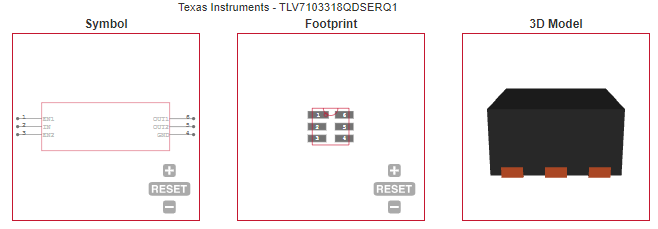
TLV7103318QDSERQ1 ECAD MODELS
|
TLV7103318QDSERQ1 APPLICATIONS
|
|
COUNTRY OF ORIGIN
|
Thailand
|
|
PARAMETRIC INFO
|
| Type |
LDO |
| Number of Outputs |
2 |
| Maximum Output Current (A) |
0.2 |
| Minimum Operating Temperature (°C) |
-40 |
| Maximum Operating Temperature (°C) |
125 |
| Output Type |
Fixed |
| Output Voltage Range (V) |
1.8 to 10 |
| Junction to Ambient |
190.5°C/W |
| Junction to Case |
94.9°C/W |
| Polarity |
Positive |
| Special Features |
Current Limit|Thermal Protection |
| Load Regulation |
15mV |
| Line Regulation |
5mV |
| Maximum Quiescent Current (mA) |
0.11 |
| Maximum Dropout Voltage @ Current (V) |
0.2@200mA |
| Minimum Input Voltage (V) |
2 |
| Maximum Input Voltage (V) |
5.5 |
| Output Voltage (V) |
1.8|3.3 |
| Typical Quiescent Current (mA) |
0.07 |
| Typical Dropout Voltage @ Current (V) |
0.14@200mA |
| Accuracy (%) |
±2 |
| Supplier Temperature Grade |
Automotive |
| Typical PSRR (dB) |
80 |
| Typical Output Capacitance (uF) |
0.1(Min) |
| Typical Output Noise Voltage (uVrms) |
48 |
|
|
PACKAGE INFO
|
| Supplier Package |
WSON |
| Basic Package Type |
Non-Lead-Frame SMT |
| Pin Count |
6 |
| Lead Shape |
No Lead |
| PCB |
6 |
| Tab |
N/R |
| Pin Pitch (mm) |
0.5 |
| Package Length (mm) |
1.55(Max) |
| Package Width (mm) |
1.55(Max) |
| Package Height (mm) |
0.75(Max) |
| Package Diameter (mm) |
N/R |
| Package Overall Length (mm) |
1.55(Max) |
| Package Overall Width (mm) |
1.55(Max) |
| Package Overall Height (mm) |
0.8(Max) |
| Seated Plane Height (mm) |
0.8(Max) |
| Mounting |
Surface Mount |
| Package Weight (g) |
N/A |
| Package Material |
Plastic |
| Package Description |
Very Very Thin Small Outline No Lead Package |
| Package Family Name |
SON |
| Jedec |
N/A |
| Package Outline |
Link to Datasheet |
|
|
MANUFACTURING INFO
|
| MSL |
1 |
| Maximum Reflow Temperature (°C) |
260 |
| Reflow Solder Time (Sec) |
30 |
| Number of Reflow Cycle |
3 |
| Standard |
J-STD-020D |
| Reflow Temp. Source |
Link to Datasheet |
| Maximum Wave Temperature (°C) |
N/R |
| Wave Solder Time (Sec) |
N/R |
| Lead Finish(Plating) |
Au |
| Under Plating Material |
Pd over Ni |
| Terminal Base Material |
Cu Alloy |
|
|
PACKAGING INFO
|
| Packaging Suffix |
R |
| Packaging |
Tape and Reel |
| Quantity Of Packaging |
3000 |
|
|
ECAD MODELS
|
|
|
| APPLICATIONS |
| • Automotive Applications |
| • Wireless Handsets, Smart Phones, PDAs |
| • MP3 Players and Other Handheld Products |
| |