 |
|
| • Low-voltage operation: down to 1.24 V
|
• Reference voltage tolerances at 25°C
– 0.5% for B grade
– 1% for A grade
– 1.5% for standard grade |
| • Adjustable output voltage, VO = VREF to 18 V |
| • Wide operating cathode current range:
100 μA to 70 mA |
| • 0.25-Ω typical output impedance |
| • –40°C to +125°C specifications |
| • TLVH432 provides alternative pinouts for
SOT-23-3 and SOT-89 packages |
| • Ultra-small SC-70 package offers 40%
smaller footprint than SOT-23-3 |
|
| CATALOG |
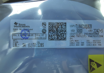
| TLVH431AQDBZR COUNTRY OF ORIGIN |
| TLVH431AQDBZR PARAMETRIC INFO |
| TLVH431AQDBZR PACKAGE INFO |
| TLVH431AQDBZR MANUFACTURING INFO |
| TLVH431AQDBZR PACKAGING INFO |
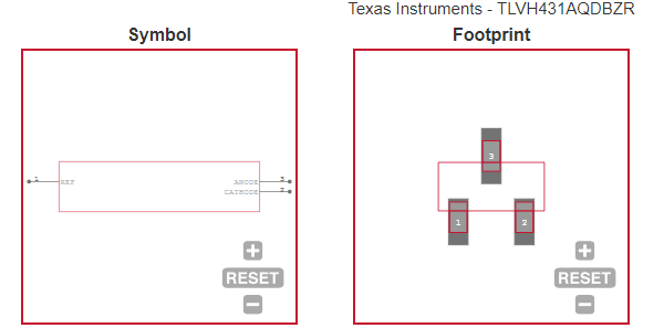
| TLVH431AQDBZR ECAD MODELS |
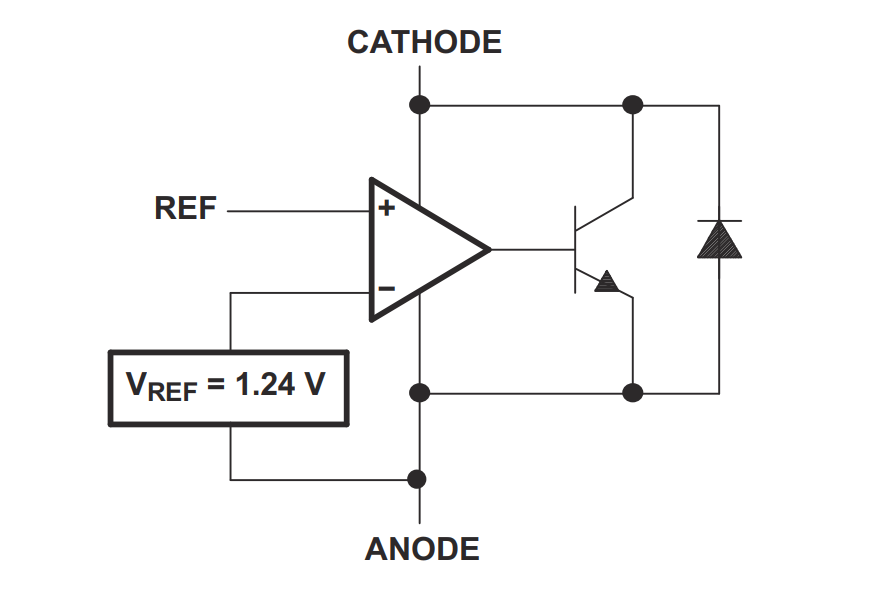
| TLVH431AQDBZR FUNCTIONAL BLOCK DIAGRAM |
| TLVH431AQDBZR APPLICATIONS |
|
| COUNTRY OF ORIGIN |
| Thailand |
| China |
| Philippines |
| Malaysia |
|
| PARAMETRIC INFO |
| Topology |
Shunt |
| Reference Type |
Adjustable |
| Output Voltage (V) |
1.24 to 18 |
| Initial Accuracy |
1% |
| Minimum Operating Temperature (°C) |
-40 |
| Maximum Operating Temperature (°C) |
125 |
| Maximum Input Voltage (V) |
20 |
| Maximum Output Current (mA) |
80 |
| Maximum Temperature Coefficient |
138ppm/°C |
|
|
| PACKAGE INFO |
| Supplier Package |
SOT-23 |
| Basic Package Type |
Lead-Frame SMT |
| Pin Count |
3 |
| Lead Shape |
Gull-wing |
| PCB |
3 |
| Tab |
N/R |
| Pin Pitch (mm) |
0.95 |
| Package Length (mm) |
3.04(Max) |
| Package Width (mm) |
1.4(Max) |
| Package Height (mm) |
0.95 |
| Package Diameter (mm) |
N/R |
| Package Overall Length (mm) |
3.04(Max) |
| Package Overall Width (mm) |
2.64(Max) |
| Package Overall Height (mm) |
1.12(Max) |
| Seated Plane Height (mm) |
1.12(Max) |
| Mounting |
Surface Mount |
| Package Weight (g) |
N/A |
| Package Material |
Plastic |
| Package Description |
Small Outline Transistor |
| Package Family Name |
SOT |
| Jedec |
TO-236AB |
| Package Outline |
Link to Datasheet |
|
|
| MANUFACTURING INFO |
| MSL |
1 |
| Maximum Reflow Temperature (°C) |
260 |
| Reflow Solder Time (Sec) |
30 |
| Number of Reflow Cycle |
3 |
| Standard |
J-STD-020D |
| Reflow Temp. Source |
Link to Datasheet |
| Maximum Wave Temperature (°C) |
260 |
| Wave Solder Time (Sec) |
4 |
| Wave Temp. Source |
Link to Datasheet |
| Lead Finish(Plating) |
Au|AuAg |
| Under Plating Material |
Pd over Ni |
| Terminal Base Material |
N/A|Cu Alloy |
| Number of Wave Cycles |
N/A |
|
|
| PACKAGING INFO |
| Packaging Suffix |
R |
| Packaging |
Tape and Reel |
| Quantity Of Packaging |
3000 |
| Reel Diameter (in) |
7.09 |
| Reel Width (mm) |
8.4 |
| Tape Pitch (mm) |
4 |
| Tape Width (mm) |
8 |
| Component Orientation |
Q3 |
| Packaging Document |
Link to Datasheet |
|
|
| ECAD MODELS |
 |
|
| FUNCTIONAL BLOCK DIAGRAM |
 |
|
| APPLICATIONS |
| • Adjustable voltage reference for data Converters |
| • Secondary side regulation in flyback SMPSs |
| • Zener replacement with low leakage current |
| • Voltage monitoring for power rails |
| • Comparator with integrated reference |
| |
|